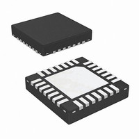
ISL62881CHRTZ Intersil, ISL62881CHRTZ Datasheet - Page 22

ISL62881CHRTZ
Manufacturer Part Number
ISL62881CHRTZ
Description
IC REG PWM SGL PHASE 28TQFN
Manufacturer
Intersil
Datasheet
1.ISL62881CHRTZ.pdf
(37 pages)
Specifications of ISL62881CHRTZ
Applications
Controller, Intel IMVP-6.5™
Voltage - Input
4.5 ~ 25 V
Number Of Outputs
1
Voltage - Output
0.0125 ~ 1.5 V
Operating Temperature
-10°C ~ 100°C
Mounting Type
Surface Mount
Package / Case
28-VQFN
For Use With
ISL62881CCPUEVAL2Z - EVAL BOARD ISL62881CCPU 28QFN
Lead Free Status / RoHS Status
Lead free / RoHS Compliant
Available stocks
Company
Part Number
Manufacturer
Quantity
Price
Part Number:
ISL62881CHRTZ
Manufacturer:
INTERSIL
Quantity:
20 000
Part Number:
ISL62881CHRTZ-T
Manufacturer:
INTERSIL
Quantity:
20 000
Substitution of Equation 28 into Equation 27 gives
Equation 29:
Rewriting Equation 29 and application of full load
condition gives Equation 30:
For example, given LL = 7mΩ, R
V
R
A capacitor C
the IMON pin voltage. The R
the user’s choice. It is recommended to have a time
constant long enough such that switching frequency
ripples are removed.
Compensator
Figure 14 shows the desired load transient response
waveforms. Figure 20 shows the equivalent circuit of a
voltage regulator (VR) with the droop function. A VR is
equivalent to a voltage source (= VID) and output
impedance Z
slope LL, i.e. constant output impedance, in the entire
frequency range, V
has a square change.
Intersil provides a Microsoft Excel-based spreadsheet to
help design the compensator and the current sensing
network, so the VR achieves constant output impedance
as a stable system. Figure 23 shows a screenshot of the
spreadsheet.
A VR with active droop function is a dual-loop system
consisting of a voltage loop and a droop loop which is a
current loop. However, neither loop alone is sufficient to
describe the entire system. The spreadsheet shows two
loop gain transfer functions, T1(s) and T2(s), that
describe the entire system. Figure 21 conceptually shows
T1(s) measurement set-up and Figure 22 conceptually
shows T2(s) measurement set-up. The VR senses the
inductor current, multiplies it by a gain of the load line
slope, then adds it on top of the sensed output voltage
and feeds it to the compensator. T(1) is measured after
the summing node, and T2(s) is measured in the voltage
loop before the summing node. The spreadsheet gives
both T1(s) and T2(s) plots. However, only T2(s) can be
actually measured on an ISL62881C regulator.
R
V
Rimon
imon
imon
Rimon
FIGURE 20. VOLTAGE REGULATOR EQUIVALENT
=
= 6.66kΩ.
= 999mV at I
=
V
----------------------------------------------
Rimon
3I
--------------------- -
R
VID
o
droop
3I
out
×
imon
o
LL
×
×
(s). If Z
R
LL
×
droop
can be paralleled with R
R
o
Z
imon
out(s)
will have square response when I
omax
out
= LL
VR
22
(s) is equal to the load line
= 22A, Equation 30 gives
imon
i
droop
O
C
imon
LOAD
= 3.08kΩ,
time constant is
ISL62881C, ISL62881D
ISL62881C, ISL62881D
imon
V
+
-
O
to filter
(EQ. 29)
(EQ. 30)
o
T1(s) is the total loop gain of the voltage loop and the
droop loop. It always has a higher crossover frequency
than T2(s) and has more meaning of system stability.
T2(s) is the voltage loop gain with closed droop loop. It
has more meaning of output voltage response.
Design the compensator to get stable T1(s) and T2(s)
with sufficient phase margin, and output impedance
equal or smaller than the load line slope.
FIGURE 21. LOOP GAIN T1(s) MEASUREMENT SET-UP
FIGURE 22. LOOP GAIN T2(s) MEASUREMENT SET-UP
V
V
IN
IN
LOOP GAIN =
LOOP GAIN =
DRIVER
DRIVER
GATE
GATE
Q1
Q1
MOD
Q2
MOD
Q2
CHANNEL B
CHANNEL A
CHANNEL B
CHANNEL A
CHANNEL A
ANALYZER
NETWORK
COMP
COMP
LOAD LINE SLOPE
ANALYZER
CHANNEL A
NETWORK
LOAD LINE SLOPE
EA
L
EA
L
+
-
+
-
VID
C
VID
EXCITATION OUTPUT
OUT
C
OUT
EXCITATION OUTPUT
V
O
+
V
20
O
+
Ω
I
O
20
I
O
Ω
+
+
ISOLATION
TRANSFORMER
CHANNEL B
ISOLATION
TRANSFORMER
March 8, 2010
CHANNEL B
FN7596.0


