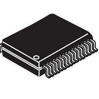
MCZ34702EWR2 Freescale Semiconductor, MCZ34702EWR2 Datasheet - Page 17

MCZ34702EWR2
Manufacturer Part Number
MCZ34702EWR2
Description
IC PWR SUPPLY 3A SW 32-SOIC
Manufacturer
Freescale Semiconductor
Datasheet
1.MC34702EK.pdf
(39 pages)
Specifications of MCZ34702EWR2
Applications
Controller, Power QUICC™ I, II
Voltage - Input
2.8 ~ 6 V
Number Of Outputs
2
Voltage - Output
7.75V, 0.8 ~ 6 V
Operating Temperature
-40°C ~ 85°C
Mounting Type
Surface Mount
Package / Case
32-SOIC (7.5mm Width)
Output Current
3 A
Input Voltage
2.8 V to 6 V
Switching Frequency
300 KHz
Mounting Style
SMD/SMT
Duty Cycle (max)
95 %
Lead Free Status / RoHS Status
Lead free / RoHS Compliant
POWER SUPPLY PIN (VDDI)
X7R capacitor is recommended.
ADDRESS PIN (ADDR)
when used in an I
tied to VDDI or grounded through a 10kΩ resistor. Refer to
I
pin.
ENABLE 1 AND 2 PINS (EN1 AND EN2)
function and selection of the Power Sequencing Mode
concurrently.
Power Sequencing Mode selection.
and both can withstand a short circuit to the supply voltage,
6.0V.
Table 5.
Analog Integrated Circuit Device Data
Freescale Semiconductor
2
C Bus Operation on page 26
Internal supply voltage. A ceramic low ESR 1uF 6V X5R or
The ADDR pin is used to set the address of the device
These two pins permit positive logic control of the Enable
Both EN1 and EN2 pins have internal pull-down resistors
EN1
0
0
1
1
Operating Mode Selection
Table 5
2
EN2
C communication. This pin can either be
0
1
0
1
depicts the EN1 and EN2 function and
for more information on this
Standard Power Sequencing
Inverted Power Sequencing
No Power Sequencing,
Regulators Disabled
Regulators Enabled
Operating Mode
RESET TIMER PIN (RT)
the delay between the time when the LDO and switcher
outputs are active and stable and the
An external resistor and capacitor are used to program the
timer. The power-up delay can be obtained by using the
following formula:
is the Reset Timer programming capacitor, both connected in
parallel from RT to ground.
accuracy if R
RESET OUTPUT PIN (
regulator and the LDO feedback voltages. It is an open drain
output and has to be pulled up to some supply voltage (e.g.,
the output of the LDO) by an external resistor.
the linear regulator output V
output V
regulation (high or low), the
20
up sequencing,
out.
CLOCK SELECTION PIN (CLKSEL)
or a synchronization input pin. The CLKSEL pin is also used
for the I
CLOCK SYNCHRONIZATION PIN (CLKSYN)
µ
The Reset Timer power-up delay (RT) pin is used to set
Where R
Note Observe the maximum C
The reset control circuit monitors both the switching
The reset control circuit supervises both output voltages—
This pin sets the CLKSYN pin as either an oscillator output
Oscillator output/synchronization input pin.
s delay filter preventing erroneous resets. During power-
2
OUT
C address selection.
t
is the Reset Timer programming resistor and C
. When either of these two regulators is out of
t
t
is less than 10kΩ.
D
RST
= 10ms + R
is held low until the Reset Timer times
RST
LDO
RST
t
FUNCTIONAL PIN DESCRIPTION
C
t
)
FUNCTIONAL DESCRIPTION
pin is pulled low. There is a
and the switching regulator
t
value and expect reduced
RST
output is released.
34702
17
t


