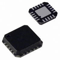
ADM8830ACP Analog Devices Inc, ADM8830ACP Datasheet - Page 2

ADM8830ACP
Manufacturer Part Number
ADM8830ACP
Description
IC CHARGE PUMP REG TFT 20LFCSP
Manufacturer
Analog Devices Inc
Datasheet
1.ADM8830ARU-REEL.pdf
(8 pages)
Specifications of ADM8830ACP
Rohs Status
RoHS non-compliant
Applications
Converter, TFT, LCD
Voltage - Input
2.6 ~ 3.6 V
Number Of Outputs
3
Voltage - Output
-10.2V, 5.1V, 15.3V
Operating Temperature
-40°C ~ 85°C
Mounting Type
Surface Mount
Package / Case
20-LFCSP
Available stocks
Company
Part Number
Manufacturer
Quantity
Price
Company:
Part Number:
ADM8830ACP
Manufacturer:
TI
Quantity:
50 000
Company:
Part Number:
ADM8830ACP-REEL7
Manufacturer:
Alpha
Quantity:
99
Part Number:
ADM8830ACP-REEL7
Manufacturer:
ADI/亚德诺
Quantity:
20 000
Part Number:
ADM8830ACPZ
Manufacturer:
ADI/亚德诺
Quantity:
20 000
Parameter
INPUT VOLTAGE, V
SUPPLY CURRENT, I
+5.1 V OUTPUT
+15.3 V OUTPUT
–10.2 V OUTPUT
POWER EFFICIENCY
CHARGE PUMP FREQUENCY
CONTROL PINS
*Guaranteed by design. Not 100% production tested.
Specifications are subject to change without notice.
ADM8830–SPECIFICATIONS
Transient Response
Output Voltage
Output Current
Power Efficiency
Output Ripple
Output Voltage
Output Current
Output Ripple
Output Voltage
Output Current
Output Ripple
(+15.3 V and –10.2 V Outputs)
SHDN
SCAN/BLANK
LDO_ON/OFF
CLKIN
Minimum Frequency
Input Voltage, V
Digital Input Current
Digital Input Capacitance*
Input Voltage
Digital Input Current
Digital Input Capacitance*
Input Voltage
Digital Input Current
Digital Input Capacitance*
Input Voltage
Digital Input Current
Digital Input Capacitance*
V
V
IL
IH
SHDN
CC
CC
Min
2.6
5.0
14.4
–10.4
–100
–10
60
0.7 V
0.7 V
0.7 V
0.9
0.7 V
CC
CC
CC
CC
Typ
150
70
5.1
4
5
50
80
70
10
5
15.3
50
1
50
–10.2
–50
–1
50
90
80
100
1
(V
C7 = 2.2 F, C2, C3, C4, C8, C9 = 1 F, CLKIN = 1 kHz in blanking mode.)
Max
3.6
400
140
1
5.2
5
8
200
15.6
100
10
–9.6
140
0.3 V
±1
10
0.3 V
±1
10
0.3 V
±1
10
0.3 V
±1
10
CC
= 2.6 V to 3.6 V, T
–2–
CC
CC
CC
CC
V
V
V
V
Unit
V
µA
µA
µA
V
mA
mA
µA
%
%
mV p-p
µs
V
µA
µA
mV p-p
V
µA
µA
mV p-p
%
%
kHz
V
µA
pF
V
µA
pF
V
µA
pF
kHz
V
µA
pF
A
= –40C to +85C, unless otherwise noted, C1, C5, C6,
Test Conditions
Unloaded, Scanning Period
Unloaded, Blanking Period
Shutdown Mode, T
I
Scanning Period
Scanning Period, V
Blanking Period
V
V
8 mA Load
I
I
Scanning Period
Blanking Period
I
I
Scanning Period
Blanking Period
I
Relative to 5.1 V Output, I
Relative to 5.1 V Output, I
Scanning Period
SHDN Low = Shutdown Mode
SHDN High = Normal Mode
Low = BLANK Period
High = SCAN Period
Low = External LDO
High = Internal LDO
Duty Cycle = 50%, Rise/Fall Times = 20 ns
L
L
L
L
L
L
CC
CC
= 10 µA to 8 mA
Stepped from 10 µA to 8 mA
= 1 µA to 100 µA
= 100 µA
= –1 µA to –100 µA
= –100 µA
= 3 V, I
= 3 V, I
L
L
= 5 mA (Scanning)
= 200 µA (Blanking)
CC
A
= 25°C
> 2.7 V
L
L
= 100 µA (Scanning)
=10 µA (Blanking)
REV. B


