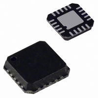
ADM8830ACP Analog Devices Inc, ADM8830ACP Datasheet - Page 7

ADM8830ACP
Manufacturer Part Number
ADM8830ACP
Description
IC CHARGE PUMP REG TFT 20LFCSP
Manufacturer
Analog Devices Inc
Datasheet
1.ADM8830ARU-REEL.pdf
(8 pages)
Specifications of ADM8830ACP
Rohs Status
RoHS non-compliant
Applications
Converter, TFT, LCD
Voltage - Input
2.6 ~ 3.6 V
Number Of Outputs
3
Voltage - Output
-10.2V, 5.1V, 15.3V
Operating Temperature
-40°C ~ 85°C
Mounting Type
Surface Mount
Package / Case
20-LFCSP
Available stocks
Company
Part Number
Manufacturer
Quantity
Price
Company:
Part Number:
ADM8830ACP
Manufacturer:
TI
Quantity:
50 000
Company:
Part Number:
ADM8830ACP-REEL7
Manufacturer:
Alpha
Quantity:
99
Part Number:
ADM8830ACP-REEL7
Manufacturer:
ADI/亚德诺
Quantity:
20 000
Part Number:
ADM8830ACPZ
Manufacturer:
ADI/亚德诺
Quantity:
20 000
SCANNING AND BLANKING
A TFT LCD panel is essentially made up of a bank of capacitors,
each representing a pixel in the display. These capacitors store
different levels of charge, depending on the amount of lumines-
cence required for a given pixel.When a picture is being displayed
on the panel, a scan of all the pixel capacitors is performed, placing
different levels of charge on each in order to create the image.The
process of updating the display like this is called “scanning.” Once
scanned, an image will be held by pixel capacitance and the con-
troller and source line drivers can be put into a low power mode.
This low power mode is referred to as the blanking mode on the
ADM8830. Over a finite period of time, this pixel charge will leak
and the capacitors will have to be refreshed in order to maintain
the image.
The ADM8830 caters to the two modes of operation described
above as follows.When the TFT LCD panel is in scanning mode,
a logic high on the SCAN/BLANK input places the device in high
current power mode, providing extra power (extra current) to the
LCD controller and the source line drivers. If the panel continues
to be updated (as when a moving picture is being displayed), then
the ADM8830 can be continually operated in scanning mode. If
the same image is kept on the panel, a logic low is applied to the
SCAN/BLANK input and the ADM8830 enters blanking (low
current) mode. Depending on how often the image is being updated,
the ADM8830 can be operated with a variable SCAN/BLANK
duty cycle.This helps to maximize power efficiency and therefore
extends the battery life.
POWER SEQUENCING
The gate drive supplies must be sequenced such that the –10 V
supply is up before the +15 V supply for the TFT panel to power
up correctly. The ADM8830 controls this sequence. When the
device is turned on (a logic high on SHDN), the ADM8830 allows
the –10 V output to ramp immediately but holds off the +15 V
output. It continues to do this until the negative output has reached
–3 V. At this point, the positive output is enabled and allowed to
ramp up to +15 V. This sequence is highlighted in Figure 2.
REV. B
t
R
Figure 1. Duty Cycle of External Clock
t
H
t
t
T
F
t
t
t
t
R
F
H
T
: FALL TIME
: RISE TIME
@ 100% = DUTY CYCLE
90%
10%
–7–
TRANSIENT RESPONSE
The ADM8830 features extremely fast transient response, making
it very suitable for fast image updates on TFT LCD panels. This
means that even under changing load conditions there is still very
effective regulation of the 5 V output. TPCs 10 and 11 show how
the 5.1 V output responds when a maximum load is dynamically
connected and disconnected. Note that the output settles within
5 µs to less than 1% of the output level.
EXTERNAL CLOCK
The ADM8830 has an internal 100 kHz oscillator, but an external
clock source can also be used to clock the part. This clock source
must be applied to the CLKIN pin. Power is saved during blank-
ing periods by disabling the internal oscillator and switching to
the lower frequency external clock source. To achieve optimum
performance of the charge pump circuitry, it is important that the
duty cycle of the external clock source be 50% and that the rise
and fall times be less than 20 ns.
BOARD METALLIZATION
EXTERNAL CLOCK
SCAN/BLANK
Figure 3. Suggested LFCSP 4 mm 4 mm 20-Lead
Land Pattern
DIMENSIONS IN
SOLDER MASK
MILLIMETERS
SHDN
LOAD
+15V
–10V
V
+5V
CC
10%
t
90%
0.5
DELAY
Figure 2. Power Sequence
t
R15V
3.10
0.75
t
F10V
t
R5V
–3V
0.28
10%
90%
0.2
ADM8830
0.4
t
F15V
0.25
0.25
0.9
1.95
t
t
F5V
R10V
2.10


