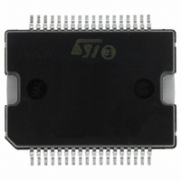
L6701 STMicroelectronics, L6701 Datasheet - Page 39

L6701
Manufacturer Part Number
L6701
Description
IC CTRLR 3PH VR10/9/K8 PWRSO-36
Manufacturer
STMicroelectronics
Datasheet
1.L6701TR.pdf
(44 pages)
Specifications of L6701
Applications
Controller, Intel VR9, VR10, K8
Voltage - Input
12V
Number Of Outputs
3
Voltage - Output
0.8 ~ 1.85 V
Operating Temperature
0°C ~ 70°C
Mounting Type
Surface Mount
Package / Case
36-PowerSOIC
Output Voltage
0.8 V to 1.85 V
Output Current
1.5 A
Switching Frequency
110 KHz
Mounting Style
SMD/SMT
Maximum Operating Temperature
+ 125 C
Minimum Operating Temperature
0 C
Lead Free Status / RoHS Status
Lead free / RoHS Compliant
Available stocks
Company
Part Number
Manufacturer
Quantity
Price
L6701
16.2
Caution:
Small Signal Components and Connections
These are small signal components and connections to critical nodes of the application as well
as bypass capacitors for the device supply (See
and Bootstrap capacitor) close to the device and refer sensible components such as frequency
set-up resistor R
a single point to avoid that drops due to the high current delivered causes errors in the device
behavior.
VSEN pin filtered vs. SGND helps in reducing noise injection into device: take care in routing
driving net for this pin in order to minimize coupled noise.
Remote Buffer Connection must be routed as parallel nets from the FBG/FBR pins to the load
in order to avoid the pick-up of any common mode noise. Connecting these pins in points far
from the load will cause a non-optimum load regulation, increasing output tolerance.
Locate current reading components close to the device. It's also important to minimize any
offset in the measurement and, to get a better precision, to connect the traces as close as
possible to the sensing elements.
Boot Capacitor Extra Charge. Systems that do not use Schottky diodes might show big
negative spikes on the phase pin. This spike can be limited as well as the positive spike but has
an additional consequence: it causes the bootstrap capacitor to be over-charged. This extra-
charge can cause, in the worst case condition of maximum input voltage and during particular
transients, that boot-to-phase voltage overcomes the abs. max. ratings also causing device
failures. It is then suggested in this cases to limit this extra-charge by:
Figure 20. Power connections and related connections layout (same for all phases).
UGATEx
PHASEx
LGATEx
PGNDx
–
–
adding a small resistor in series to the boot diode (one resistor can be enough for all
the three diodes if placed upstream the boot diode anode, see
using non-capacitive boot diodes (such as standard diodes).
OSC
to SGND. Star grounding is suggested: connect SGND to PGND plane in
V
C
IN
IN
L
LOAD
PHASEx
Figure
BOOTx
SGND
VCC
To limit C
20). Locate the bypass capacitor (VCC
BOOT
Extra-Charge
+Vcc
Figure
V
C
IN
IN
16 Layout Guidelines
L
20)
39/44
LOAD


