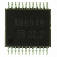
AN8049SH-E1 Panasonic - SSG, AN8049SH-E1 Datasheet - Page 10

AN8049SH-E1
Manufacturer Part Number
AN8049SH-E1
Description
IC MULTI CONFIG 40MA SSOP24D
Manufacturer
Panasonic - SSG
Type
Step-Down (Buck), Step-Up (Boost), Invertingr
Specifications of AN8049SH-E1
Internal Switch(s)
Yes
Synchronous Rectifier
No
Number Of Outputs
3
Current - Output
40mA
Frequency - Switching
20kHz ~ 1MHz
Voltage - Input
1.8 ~ 14 V
Operating Temperature
-30°C ~ 85°C
Mounting Type
Surface Mount
Package / Case
24-SSOP
Power - Output
146mW
Lead Free Status / RoHS Status
Contains lead / RoHS non-compliant
Voltage - Output
-
Other names
AN8049SHE1
AN8049SHE1TR
AN8049SHE1TR
Available stocks
Company
Part Number
Manufacturer
Quantity
Price
Company:
Part Number:
AN8049SH-E1V
Manufacturer:
MITSUMI
Quantity:
2 511
Part Number:
AN8049SH-E1V
Manufacturer:
PANASONIC/松下
Quantity:
20 000
AN8049FHN
I Terminal Equivalent Circuits (continued)
I Usage Notes
10
[1] Allowable power dissipation
Pin No.
careful to operate so that the loss does not exceed the allowable power dissipation, P
23
24
Since the power dissipation (P) in this IC increases proportionally with the supply voltage, applications must be
Reference formula:
P = (V
< P
+ (V
+ V
+ V
V
I
Du
V
I
Du
V
I
Du
I
SO(OUT)1
SO(OUT)2
OUT3
CC
D
1.5 kΩ
BEQ1
BEQ2
O(SAT)3
CC
1
2
3
O(SAT)3
CC
CC
− V
× I
50 kΩ
− V
23
24
BEQ1
CC
Equivalent circuit
: The voltage between the base and emitter of the npn transistor Q1
: The OUT1 pin output source current
: The output 1 duty factor
: The voltage between the base and emitter of the npn transistor Q2
: The OUT2 pin output source current
: The output 2 duty factor
: The OUT3 pin saturation voltage (0.5 V maximum when OUT1 is 40 mA.)
: The OUT3 pin current (This will be {V
: The output 3 duty factor
: The V
1.1 µA
× I
(When R
(When R
BEQ2
7 18 15
) × I
OUT3
1.26 V
V
50 kΩ
) × I
CC
CC
SO(OUT)1
× Du
SO(OUT)2
RB1
RB2
pin current
Latch
S
R
is 1 kΩ, I
is 1 kΩ, I
3
PWM3
Q
× Du
× Du
Output
shutoff
1
SO(OUT)1
SO(OUT)2
2
SDH000011BEB
← Power dissipation in the channel 1 output stage
← Power dissipation in the channel 2 output stage
← Power dissipation in the channel 3 output stage
← Power dissipation between V
will be 38 mA, maximum.)
will be 38 mA, maximum.)
S.C.P.:
Connection for the capacitor that sets the timer
latch short-circuit protection circuit time
constant. Use a capacitor with a value of 1 000
pF or higher.
The charge current I
DT3:
Sets the channel 3 soft start time.
Set the time by connecting a capacitor between
this pin and ground. Note that although the
channel 3 maximum on duty is set internally to
86%, the maximum on duty can be set to a value
of 86% or less by inserting a resistor between
this pin and ground, and can be set to a value of
86% or more by inserting a resistor between this
pin and the V
CC
− V
BEQ3
REF
− V
Description
pin.
CHG
O(SAT)3
is 1.1 µA typical.
CC
D
}/R
and ground
, for the package.
O3
.)
I/O
O
I


