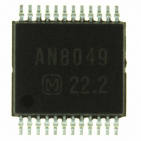
AN8049SH-E1 Panasonic - SSG, AN8049SH-E1 Datasheet - Page 14

AN8049SH-E1
Manufacturer Part Number
AN8049SH-E1
Description
IC MULTI CONFIG 40MA SSOP24D
Manufacturer
Panasonic - SSG
Type
Step-Down (Buck), Step-Up (Boost), Invertingr
Specifications of AN8049SH-E1
Internal Switch(s)
Yes
Synchronous Rectifier
No
Number Of Outputs
3
Current - Output
40mA
Frequency - Switching
20kHz ~ 1MHz
Voltage - Input
1.8 ~ 14 V
Operating Temperature
-30°C ~ 85°C
Mounting Type
Surface Mount
Package / Case
24-SSOP
Power - Output
146mW
Lead Free Status / RoHS Status
Contains lead / RoHS non-compliant
Voltage - Output
-
Other names
AN8049SHE1
AN8049SHE1TR
AN8049SHE1TR
Available stocks
Company
Part Number
Manufacturer
Quantity
Price
Company:
Part Number:
AN8049SH-E1V
Manufacturer:
MITSUMI
Quantity:
2 511
Part Number:
AN8049SH-E1V
Manufacturer:
PANASONIC/松下
Quantity:
20 000
AN8049FHN
I Application Notes (continued)
14
[4] Function descriptions
1. Reference voltage block
2. Triangular wave generator
3. Error amplifier 1
4. Error amplifier 2
temperature compensated to a precision of ±1%. This reference voltage is stabilized when the supply voltage is 1.8
V or higher. This reference voltage is used by error amplifiers 1 and 2.
with a peak of 0.7 V and a trough of 0.2 V using a capacitor
C
pin (pin 15). The oscillator frequency can be set to an arbi-
trary value by selecting appropriate values for the external ca-
pacitor and resistor, C
frequency in the range 20 kHz to 1 MHz. The triangular wave
signal is provided to the noninverting input of the PWM com-
parator in each channel internally to the IC. Use the formulas
below for rough calculation of the oscillator frequency.
account. See the experimentally determined graph of the oscillator frequency vs. timing capacitance value pro-
vided in the main characteristics section.
that detects and amplifies the DC-DC converter output
voltage, and inputs that signal to a PWM comparator.
The 1.26 V internal reference voltage is applied to the
noninverting input. Arbitrary gain and phase compensa-
tion can be set up by inserting a resistor and capacitor in
series between the FB1 pin (pin 22) and the IN−1 pin
(pin 21). The output voltage V
circuit shown in the figure.
that detects and amplifies the DC-DC converter output
voltage, and inputs that signal to a PWM comparator.
The 1.26 V internal reference voltage is applied to the
noninverting input. Arbitrary gain and phase compensa-
tion can be set up by inserting a resistor and capacitor in
series between the FB2 pin (pin 20) and the IN−2 pin
(pin 19). The output voltage V
circuit shown in the figure.
T
(for the time constant) and resistor R
This circuit is composed of a band gap circuit, and outputs a 1.26 V (typical) reference voltage that is
This circuit generates a triangular wave like a sawtooth
f
Note, however, that the above formulas do not take the rapid charge time, overshoot, and undershoot into
This circuit is an npn-transistor input error amplifier
This circuit is an npn-transistor input error amplifier
OSC
≈ −
C
T
× R
T
T
× ln
1
and R
V
V
OSCL
OSCH
T
OUT2
OUT1
. This IC can use an oscillator
≈ 0.8 ×
can be set using the
can be set using the
T
connected to the OSC
C
SDH000011BEB
T
× R
1
T
(Hz)
Figure 3. Connection method of error amplifier 2
R1
R2
R1
R2
Figure 2. Connection method of error amplifier 1
V
V
OUT1
OUT2
charge
Rapid
Figure 1. Triangular oscillator waveform
t
V
V
1
OUT1
OUT2
FB2
FB1
IN−1
IN−2
(Step-up output)
(Step-up output)
= 1.26 ×
= 1.26 ×
22
21
20
19
Discharge
Error
amplifier 2
Error
amplifier 1
T
t
2
1.26 V
1.26 V
R
R
1
1
R
R
+ R
+ R
2
2
2
2
To the PWM
comparator input
To the PWN
comparator input
V
≈ 0.7 V
V
≈ 0.2 V
OSCH
OSCL


