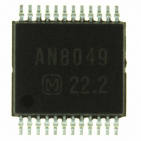
AN8049SH-E1 Panasonic - SSG, AN8049SH-E1 Datasheet - Page 15

AN8049SH-E1
Manufacturer Part Number
AN8049SH-E1
Description
IC MULTI CONFIG 40MA SSOP24D
Manufacturer
Panasonic - SSG
Type
Step-Down (Buck), Step-Up (Boost), Invertingr
Specifications of AN8049SH-E1
Internal Switch(s)
Yes
Synchronous Rectifier
No
Number Of Outputs
3
Current - Output
40mA
Frequency - Switching
20kHz ~ 1MHz
Voltage - Input
1.8 ~ 14 V
Operating Temperature
-30°C ~ 85°C
Mounting Type
Surface Mount
Package / Case
24-SSOP
Power - Output
146mW
Lead Free Status / RoHS Status
Contains lead / RoHS non-compliant
Voltage - Output
-
Other names
AN8049SHE1
AN8049SHE1TR
AN8049SHE1TR
Available stocks
Company
Part Number
Manufacturer
Quantity
Price
Company:
Part Number:
AN8049SH-E1V
Manufacturer:
MITSUMI
Quantity:
2 511
Part Number:
AN8049SH-E1V
Manufacturer:
PANASONIC/松下
Quantity:
20 000
I Application Notes (continued)
[4] Function descriptions (continued)
R1
R2
5. Error amplifier 3
6. Timer latch short-circuit protection circuit
7. Low input voltage malfunction prevention circuit (U.V.L.O.)
8. PWM comparators
V
REF
V
voltage and inputs that signal to a PWM comparator. Arbitrary gain and phase compensation can be set up by
inserting a resistor and capacitor in series between the FB3 pin (pin 18) and the IN−3 pin (pin 17). The output voltage
V
against degradation or destruction if an excessive load or a short circuit of the power supply output continues for
longer than a certain fixed period.
output voltage drops and an FB pin (pins 18, 20, or 22) voltage exceeds 0.9 V, the S.C.P. comparator outputs a low
level and the timer circuit starts. This starts charging the external protection circuit delay time capacitor.
the latch circuit latches, the output drive transistors are turned off, and the dead-time is set to 100%.
power supply voltage falls during power on or power off.
the supply voltage level. While the supply voltage is rising, this circuit cuts off the output drive transistor until the
reference voltage reaches 1.67 V. It also sets the dead-time to 100% and at the same time holds the S.C.P. pin (pin
23) and the DT pins (pins 1, 2, and 24) at 0 V, and the OSC pin (pin 15) at about 1.2 V.
both of the corresponding FB pin (pins 18, 20, or 22) and the corresponding DT pin (pins 1, 2, or 24).
a higher level than both of the FB2 pin (pin 20) and the DT2 pin (pin 1).
between the corresponding DT pin and ground, and can be set to a value higher than 86% by inserting a resistor
between the corresponding DT pin and the V
startup if a capacitor is inserted between the DT pin and ground.
R3
R4
OUT3
OUT3
V
This circuit is a pnp-transistor input error amplifier that detects and amplifies the DC-DC converter output
This circuit protects the external main switching elements, flywheel diodes, choke coils, and other components
The timer latch short-circuit protection circuit detects the output of the error amplifiers. If the DC-DC converter
If the error amplifier output does not return to the normal voltage range before that capacitor reaches 1.26 V,
This circuit protects the system against degradation or destruction due to incorrect control operation when the
The low input voltage malfunction prevention circuit detects the internal reference voltage that changes with
The PWM comparators control the on-period of the output pulse according to their input voltage.
The output transistors are turned on during periods when the OSC pin (pin 15) triangular wave is lower than
The PWM 2 circuit turns the output transistor on during periods when OSC pin (pin 15) triangular wave is at
The maximum duty is set to 86% internally, but it can be set to a value lower than 86% by inserting a resistor
The IC's soft start function operates to gradually increase the width of the output pulse on-period during
OUT3
can be set using the circuit shown in the figure.
=
R
1
R
+ R
2
Step-down output
FB3
IN+3
IN−3
2
×
R
18
16
17
3
Error
amplifier 3
R
+ R
4
4
Figure 4. Connection method of error amplifier 3
× V
REF
To the PWM
comparator input
REF
SDH00011BEB
pin.
R1
R2
V
V
OUT3
REF
V
OUT3
Inverting output
FB3
IN+3
IN−3
= −V
18
16
17
Error
amplifier 3
REF
×
R
R
2
1
AN8049FHN
To the PWM
comparator input
15


