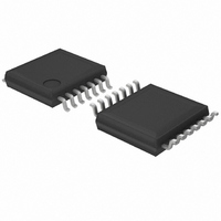
BD9845FV-E2 Rohm Semiconductor, BD9845FV-E2 Datasheet - Page 14

BD9845FV-E2
Manufacturer Part Number
BD9845FV-E2
Description
IC REG SW STEP DOWN 1CH 14-SSOP
Manufacturer
Rohm Semiconductor
Type
Step-Down (Buck)r
Datasheet
1.BD9845FV-E2.pdf
(16 pages)
Specifications of BD9845FV-E2
Internal Switch(s)
No
Synchronous Rectifier
No
Number Of Outputs
1
Current - Output
1A
Frequency - Switching
100kHz ~ 1.5MHz
Voltage - Input
3.6 ~ 35 V
Operating Temperature
-40°C ~ 85°C
Mounting Type
Surface Mount
Package / Case
14-SSOP
Power - Output
500mW
Lead Free Status / RoHS Status
Lead free / RoHS Compliant
Voltage - Output
-
Lead Free Status / Rohs Status
Lead free / RoHS Compliant
Other names
BD9845FV-E2TR
●Notes for use
© 2009 ROHM Co., Ltd. All rights reserved.
BD9845FV
www.rohm.com
1) About maximum absolute rating
2) GND potential
3) Thermal design
4) Shorting between terminals and wrong attachment
5) Operation in intense magnetic field
6) Inspection on set board
7) About IC terminal input
When the maximum absolute rating of application voltage or operation voltage range is exceeded, it may lead to
deterioration or rupture. It is impossible to forecast rupture in short mode or open mode. When a special mode is expected
exceeding the maximum absolute rating, try to take a physical safety measure such as a fuse.
Ensure that the potential of GND terminal is the minimum in any operation condition. Also ensure that no terminal except
GND terminal has a voltage below GND voltage including actual transient phenomenon.
Allow a sufficient margin in thermal design in consideration of permissible loss (Pd) in actual use condition.
When attaching an IC to a set board, pay full attention to the direction of IC and dislocation. Wrong attachment may cause
rupture of IC. In addition, when shorting is caused by foreign substance placed between outputs or between output and
power supply-GND, rupture is also possible.
Use in intense magnetic field may result in malfunction. Be careful.
In inspection on set board, when a capacitor is connected to a terminal with low impedance, stress may be applied to IC,
therefore be sure to discharge electricity in each process. Apply grounding to assembling process for a measure against
static electricity, and take enough care in transport and storage. When connecting a jig in inspection process, be sure to
turn off power before detaching IC.
This IC is a monolithic IC, and contains P
P-layer and N-layer of each element form P-N junction, and many kinds of parasitic elements are constituted. (See Fig 43.)
For example, when resistor and transistor are connected with a terminal as shown below.
Parasitic element is inevitably generated by potential because of IC structure. Operation of parasitic element causes
interference with circuit operation, and may lead to malfunction, and also may cause rupture. Therefore when applying a
voltage lower than GND (P board) to I/O terminal, pay full attention to usage so that parasitic elements do not operate.
○P-N junction operates as a parasitic diode when
○In addition, when GND>(Terminal B) for transistor (NPN),
GND>(Terminal A) for resistor, and when GND>(Terminal B) for transistor (NPN).
parasitic NPN transistor is operated by N-layer of some other elements in the vicinity of parasitic diode mentioned above.
(Terminal A)
(端子A)
(Terminal A)
N
(端子A)
P
+
P board
P基板
Resistor
GND
抵抗
GND
N
寄生素子
Parasitic element
P
Parasitic element
寄生素子
+
isolation and P board for separating elements between each element. This
P
+
Fig.44
N
14/15
Another element in
the vicinity
近接する他の素子
(端子B)
(Terminal B)
(Terminal B)
N
Parasitic element
(端子B)
P
+
寄生素子
C
Transistor (NPN)
トランジスタ(NPN)
P board
B
P基板
GND
N
N
E
B
P
E
C
GND
P +
Parasitic element
寄生素子
N
GND
2009.05 - Rev.A
Technical Note


