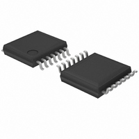
BD9845FV-E2 Rohm Semiconductor, BD9845FV-E2 Datasheet - Page 9

BD9845FV-E2
Manufacturer Part Number
BD9845FV-E2
Description
IC REG SW STEP DOWN 1CH 14-SSOP
Manufacturer
Rohm Semiconductor
Type
Step-Down (Buck)r
Datasheet
1.BD9845FV-E2.pdf
(16 pages)
Specifications of BD9845FV-E2
Internal Switch(s)
No
Synchronous Rectifier
No
Number Of Outputs
1
Current - Output
1A
Frequency - Switching
100kHz ~ 1.5MHz
Voltage - Input
3.6 ~ 35 V
Operating Temperature
-40°C ~ 85°C
Mounting Type
Surface Mount
Package / Case
14-SSOP
Power - Output
500mW
Lead Free Status / RoHS Status
Lead free / RoHS Compliant
Voltage - Output
-
Lead Free Status / Rohs Status
Lead free / RoHS Compliant
Other names
BD9845FV-E2TR
© 2009 ROHM Co., Ltd. All rights reserved.
BD9845FV
www.rohm.com
7) STB /SEL(Standby/Master/Slave function)
8) OUT (Output: External FET gate drive)
9) Protection (other protection functions)
Master mode and slave mode can be switched by SEL terminal (10pin).
1.
2.
Standby mode and normal mode can be switched by STB terminal (4pin).
1.
2.
OUT terminal (6pin) is capable of directly driving the gate of
external (PchMOS) FET. Amplitude of output is restricted
between Vcc and C5V (Vcc-5V), and is not restricted by
voltage resistance of gate by input voltage, which allows
broad selection of FET.
However, for precaution when selecting FET, there is a
restriction that input capacity of gate is determined by
current capability of C5V and permissible loss of IC,
therefore refer to the permissible range in the graph on the
right when determining FET.
This IC is equipped with low input malfunction prevention circuit (UVLO) and abnormal temperature protection circuit
(TSD) in addition to overcurrent detection circuit (OCP).
Low input malfunction prevention circuit is for preventing unstable output when input voltage is low.
Three positions of Vcc (3.2V), VREF(2.35V), and C5V(Vcc-3V) are monitored, and output is made only when all are
canceled. (See the timing chart.)
Abnormal temperature protection circuit is for protecting IC chip from destruction for preventing runaway when abnormal
heating is caused on IC exceeding rated temperature. (It does not operate normally.)
Apply a design with full margin allowed for heating in consideration of permissible loss.
When STB<0.5V, standby mode is set.
Out put stop (OUT=H) and REG also stops. Circuit current is also Isc = 0 uA here.
When STB>3.0V, normal operation mode is set.
All circuits operate. Use the controller normally in this range.
Operation status is set , but OSC block alone is stopped, CT terminal is High-Z here, and triangular wave is not
output.(PWM circuit and protection circuit perform the same operation as usual.) Therefore, if the controller is used in
this more without using master IC, triangular wave is not emitted, operation is unstable, and normal output cannot be
obtained. Be careful.
When SEL<0.5V, master mode is set.
All circuits operate.
When SEL>0.5V, slave mode is set.
9/15
1.E-07
1.E-08
1.E-09
1.E-10
100
Permissible range
Area below each line under each condition
Fig.35 OUT 端子外付け容量許容範囲
Switching f requency [kHz]
Fig.36
1000
2009.05 - Rev.A
Technical Note
Cout_max
Cout_max
(Vcc=10V)
Cout_max
(Vcc=20V)
Cout_max
(Vcc=30V)
10000


