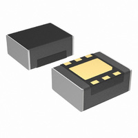
XCL206B283AR-G Torex Semiconductor Ltd, XCL206B283AR-G Datasheet - Page 17

XCL206B283AR-G
Manufacturer Part Number
XCL206B283AR-G
Description
IC BUCK SYNC 2.8V 0.6A USP-6EL
Manufacturer
Torex Semiconductor Ltd
Series
XCL206r
Type
Point of Load (POL) Non-Isolated with UVLOr
Datasheet
1.XCL206B123AR-G.pdf
(27 pages)
Specifications of XCL206B283AR-G
Output
2.8V
Number Of Outputs
1
Power (watts)
1W
Mounting Type
Surface Mount
Voltage - Input
2 ~ 6 V
Package / Case
USP-6EL
1st Output
2.8 VDC @ 600mA
Size / Dimension
0.10" L x 0.08" W x 0.04" H (2.5mm x 2.0mm x 1.04mm)
Power (watts) - Rated
1W
Operating Temperature
-40°C ~ 85°C
Efficiency
90%
Current - Output
600mA
Voltage - Output
2.8V
Power - Output
1W
Internal Switch(s)
Yes
Frequency - Switching
3MHz
Synchronous Rectifier
Yes
For Use With
893-1159 - BOARD EVAL XCL206B283AR-G 2.8V
Lead Free Status / RoHS Status
Lead free / RoHS Compliant
Other names
893-1151-2
■NOTE ON USE
1. The XCL205/XCL206/XCL207 series is designed for use with ceramic output capacitors. If, however, the potential
2. Spike noise and ripple voltage arise in a switching regulator as with a DC/DC converter. These are greatly influenced by
3. Depending on the input-output voltage differential, or load current, some pulses may be skipped, and the ripple voltage may
4. When the difference between V
5. When the difference between V
6. With the IC, the peak current of the coil is controlled by the current limit circuit. Since the peak current increases when
7. When the peak current which exceeds limit current flows within the specified time, the built-in P-ch driver transistor turns off.
8. When V
9. Depending on the state of the PC Board, latch time may become longer and latch operation may not work. In order to avoid
10. Use of the IC at voltages below the recommended voltage range may lead to instability.
11. This IC should be used within the stated absolute maximum ratings in order to prevent damage to the device.
12. When the IC is used in high temperature, output voltage may increase up to input voltage level at no load because of the
13. The current limit is set to 1350mA (MAX.) at typical. However, the current of 1350mA or more may flow. In case that the
difference is too large between the input voltage and the output voltage, a ceramic capacitor may fail to absorb the resulting
high switching energy and oscillation could occur on the output. If the input-output potential difference is large, connect an
electrolytic capacitor in parallel to compensate for insufficient capacitance.
external component selection, such as the coil inductance, capacitance values, and board layout of external components.
Once the design has been completed, verification with actual components should be done.
increase.
possibility that some cycles may be skipped completely.
there is the possibility that some cycles may be skipped completely.
dropout voltage or load current is high, current limit starts operation, and this can lead to instability. When peak current
becomes high, please adjust the coil inductance value and fully check the circuit operation. In addition, please calculate
the peak current according to the following formula:
During the time until it detects limit current and before the built-in transistor can be turned off, the current for limit current
flows; therefore, care must be taken when selecting the rating for the external components such as a coil.
the effect of noise, the board should be laid out so that input capacitors are placed as close to the IC as possible.
①Current flows into P-ch MOSFET to reach the current limit (I
⑤The circuit is latched, stopping its operation.
②The current of I
③Because of no potential difference at both ends of the coil, the time rate of coil current becomes quite small.
④Lx oscillates very narrow pulses by the current limit for several ms.
Ipk = (V
L: Coil Inductance Value
f
leak current of the driver transistor.
OSC
current limit functions while the V
input voltage will occur at both ends of a coil. For this, the time rate of coil current becomes large. By contrast, when
N-ch MOSFET is ON, there is almost no potential difference at both ends of the coil since the V
GND pin. Consequently, the time rate of coil current becomes quite small. According to the repetition of this operation,
and the delay time of the circuit, coil current will be converged on a certain current value, exceeding the amount of current,
which is supposed to be limited originally. Even in this case, however, after the over current state continues for several
ms, the circuit will be latched. A coil should be used within the stated absolute maximum rating in order to prevent
damage to the device.
OFF of P-ch MOSFET.
: Oscillation Frequency
IN
IN
is less than 2.4V, limit current may not be reached because voltage falls caused by ON resistance.
- V
OUT
I
Lx
ILx
LIM
) x OnDuty / (2 x L x f
LIM
or more flows since the delay time of the circuit occurs during from the detection of the current limit to
①
IN
IN
and V
and V
OUT
②
Duty
OSC
pin is shorted to the GND pin, when P-ch MOSFET is ON, the potential difference for
③
OUT
OUT
) + I
is small, and the load current is heavy, very wide pulses will be outputted and
is large in PWM control, very narrow pulses will be outputted, and there is the
OUT
Limit > # ms
LIM
④
).
⑤
XCL205/XCL206/XCL207
OUT
pin is shorted to the
17/27
Series


