BD9703FP-E2 Rohm Semiconductor, BD9703FP-E2 Datasheet - Page 3
BD9703FP-E2
Manufacturer Part Number
BD9703FP-E2
Description
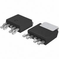
IC REG SW W/MOSFET 1CH TO252-5
Manufacturer
Rohm Semiconductor
Type
Step-Down (Buck)r
Datasheet
1.BD9703FP-E2.pdf
(17 pages)
Specifications of BD9703FP-E2
Internal Switch(s)
Yes
Synchronous Rectifier
No
Number Of Outputs
1
Voltage - Output
1 ~ 32 V
Current - Output
1.5A
Frequency - Switching
300kHz
Voltage - Input
8 ~ 36 V
Operating Temperature
-40°C ~ 85°C
Mounting Type
Surface Mount
Package / Case
DPak, TO-252 (4 leads + tab)
Power - Output
800mW
Primary Input Voltage
35V
No. Of Outputs
1
Output Voltage
32V
Output Current
1.5A
Voltage Regulator Case Style
TO-252
No. Of Pins
5
Operating Temperature Range
-40°C To +85°C
Svhc
No SVHC (18-Jun-2010)
Lead Free Status / RoHS Status
Lead free / RoHS Compliant
Lead Free Status / RoHS Status
Lead free / RoHS Compliant, Lead free / RoHS Compliant
Other names
BD9703FP-E2TR
Available stocks
Company
Part Number
Manufacturer
Quantity
Price
Company:

Part Number:
BD9703FP-E2
Manufacturer:
ROHM
Quantity:
1 250
Company:
Part Number:
BD9703FP-E2
Manufacturer:
ROHM
Quantity:
7 082
Part Number:
BD9703FP-E2
Manufacturer:
ROHM/罗姆
Quantity:
20 000


●Electrical Characteristics
●Electrical Characteristics
© 2009 ROHM Co., Ltd. All rights reserved.
BD9701FP/CP-V5/T/T-V5,BD9703FP/CP-V5/T/T-V5,BD9702CP-V5/T/T-V5
www.rohm.com
○BD9703FP/CP-V5/T/T-V5 (Unless otherwise noted, Ta=25℃,VCC=12V,Vo=5V,STBY=3V)
○BD9702FP/CP-V5/T/T-V5 (Unless otherwise noted, Ta=25℃,VCC=12V,Vo=5V,STBY=3V)
Output ON Resistance
Efficiency
Switching Frequency
Load Regulation
Line Regulation
Over Current Protection Limit
INV Pin Threshold Voltage
INV Pin Threshold Voltage
Thermal Variation
INV Pin Input Current
STBY Pin
Threshold Voltage
STBY Pin Input Current
Circuit Current
Stand-by Current
Output ON Resistance
Efficiency
Switching Frequency
Load Regulation
Line Regulation
Over Current Protection Limit
INV Pin Threshold Voltage
INV Pin Threshold Voltage
Thermal Variation
INV Pin Input Current
STBY Pin
Threshold Voltage
STBY Pin Input Current
Circuit Current
Stand-by Current
Parameter
Parameter
OFF
OFF
ON
ON
VSTBYOFF
VSTBYOFF
ΔVOLOAD
VSTBYON
ΔVOLOAD
VSTBYON
ΔVOLINE
ΔVOLINE
Symbol
Symbol
ΔVINV
ΔVINV
VINV
VINV
Istby
Istby
Ron
fosc
Iocp
IINV
Ron
fosc
Iocp
IINV
Icc
Icc
Ist
Ist
η
η
3/16
0.98
0.98
MIN
MIN
270
-0.3
-0.3
1.6
2.0
3.2
2.0
88
5
5
-
-
-
-
-
-
-
-
-
-
-
-
-
-
-
-
Limit
Limit
TYP
1.00
±0.5
TYP
1.00
±0.5
300
110
1.0
0.5
86
10
40
25
86
10
40
25
1
5
0
1
4
0
-
-
-
-
-
-
MAX
MAX
1.02
1.02
100
132
100
330
1.5
0.3
1.5
0.3
40
36
50
12
40
36
50
12
5
5
-
-
-
-
-
-
-
-
Unit
kHz
Unit
kHz
mV
mV
mA
mV
mV
mA
μA
μA
μA
μA
μA
μA
%
%
%
%
Ω
Ω
A
V
V
V
A
V
V
V
design guarantee
Io=0.5A design guarantee
VCC=20V,Io=0.5~1.5A
VCC=10~30V,Io=1.0A
Tj=0~85℃ design guarantee
VINV=1.0V
STBY=3V
STBY=0V
design guarantee
Io=1A design guarantee
VCC=20V,Io=1~3A
VCC=10~30V,Io=1.0A
Tj=0~85℃ design guarantee
VINV=1.0V
STBY=3V
STBY=0V
Conditions
Conditions
Technical Note
2009.04- Rev.B
Related parts for BD9703FP-E2
Image
Part Number
Description
Manufacturer
Datasheet
Request
R

Part Number:
Description:
Manufacturer:
Rohm Semiconductor
Datasheet:
Part Number:
Description:
Manufacturer:
Rohm Semiconductor
Datasheet:
Part Number:
Description:
Manufacturer:
Rohm Semiconductor
Datasheet:
Part Number:
Description:
Manufacturer:
Rohm Semiconductor
Datasheet:
Part Number:
Description:
Manufacturer:
Rohm Semiconductor
Datasheet:
Part Number:
Description:
Manufacturer:
Rohm Semiconductor
Datasheet:
Part Number:
Description:
Manufacturer:
Rohm Semiconductor
Datasheet:
Part Number:
Description:
Manufacturer:
Rohm Semiconductor
Datasheet:
Part Number:
Description:
Manufacturer:
Rohm Semiconductor
Datasheet:
Part Number:
Description:
Manufacturer:
Rohm Semiconductor
Datasheet:
Part Number:
Description:
Manufacturer:
Rohm Semiconductor
Datasheet:
Part Number:
Description:
Manufacturer:
Rohm Semiconductor
Datasheet:

Part Number:
Description:
DIODE SWITCH 80V 25MA SMD5 TR
Manufacturer:
Rohm Semiconductor
Datasheet: