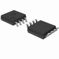
BD9850FVM-TR Rohm Semiconductor, BD9850FVM-TR Datasheet

BD9850FVM-TR
Specifications of BD9850FVM-TR
Available stocks
Related parts for BD9850FVM-TR
BD9850FVM-TR Summary of contents
Page 1
... The BD9850FVM is a 1-channel DC/DC step-down switching regulator controller, while the BD9851EFV is a 2-channel DC/DC step-down switching regulator controller. The BD9850FVM is adaptable for a maximum switching frequency of 2 MHz and the BD9851EFV for that of 3 MHz. Both provide space saving in all applications. ...
Page 2
... Between OUT1, OUT2 and PGND Power dissipation Operating temperature Maximum junction temperature Storage temperature * ( )Reduce by 8.0 mW/ ºC over 25ºC (When mounted on PCB of 70mm×70mm×1.6mm) Recommended operating range BD9850FVM Item Power supply voltage Oscillation frequency Operating temperature BD9851EFV Item Power supply voltage Oscillation frequency ...
Page 3
... BD9850FVM Electrical characteristics (Unless otherwise specified, Ta=25˚C, Vcc=7V, fosc=600kHz) Item [Oscillator block] Oscillation frequency Frequency regulation Oscillator amplitude voltage [Soft start / SW block] CTL/ SS pin sink current CTL / SS pin clamp voltage CTL threshold voltage VCTLTH [PWM comparator block] 0% threshold voltage 100% threshold voltage ...
Page 4
BD9851EFV Electrical characteristics (Unless otherwise specified, Ta=25˚C, Vcc=12V, fosc=300kHz, STB=3V) Item [Total device] Standby mode circuit current Operation mode circuit current [Reference voltage block] Output voltage Input stability Load stability Short circuit mode output current [Oscillator block] Oscillation frequency Oscillation ...
Page 5
... Characteristic data (BD9850FVM) 1.02 1.015 1.01 1.005 1 0.995 0.99 0.985 0.98 –40 – AMBIENT TEMPERATURE : Ta(˚C) Fig.1 Error Amp threshold voltage vs. Ambient temperature 1000 900 800 700 600 500 400 300 200 100 0 0 0.25 0.5 0.75 1 1.25 (V -OUT)VOLTAGE : VO(V) CC Fig.3 (Vcc-OUT) Voltage vs. Output source current 2 ...
Page 6
AMBIENT TEMPERATURE : Ta(˚C) Fig.7 Error Amp threshold voltage vs. Ambient temperature 1000 Vcc=20V 900 800 700 600 500 400 300 200 100 0 0 0.5 ...
Page 7
... Fig.14 BD9851EFV Block diagram Vcc Vcc V RT REF REF TRI Clamper V REF PWM COMP 7 CTL/SS Fig.13 BD9850FVM Block diagram Pin No. Pin name Power supply 1 Vcc 2 OUT FET driver drive output 3 GND Ground 4 V Reference voltage (2.5V±1%) output REF 5 INV Error Amp inverting input ...
Page 8
... GND pins recommended to use a ceramic capacitor of 1μF for this purpose. REF Triangular wave oscillator block 2) By connecting the resistor and capacitor of frequency settings to the RT and CT pins (only to RT pin on the BD9850FVM), a triangular wave will be generated and then input to the PWM comparators of Channels 1 and 2. Error Amp block 3) The Error Amp block detects the output voltage of the INV pin, amplifies an error with the set output voltage, and then outputs the error from the FB pin. The comparison voltage with a ± ...
Page 9
... Vcc pin voltage waveform 3.8V SCP pin voltage waveform OUT pin voltage waveform Output voltage waveform FB pin voltage Soft start set voltage Oscillator output Fig.15 BD9850FVM Timing chart Output short circuit FB CT DTC 2.3V Fig.16 BD9851EFV Timing chart 9/16 1.5V ...
Page 10
... Description of external components • Setting of output voltage (BD9850FVM) Setting of output voltage for the step-down application can be calculated by the formula below : Setting procedure Vo = Vthea × ( [V] (Vthea: Error Amp threshold voltage Typ. 1.0 [V]) Setting of output voltage (BD9851EFV) Setting procedure • Step-down (CH1), Step-up (CH1) Vo1 = Vthea × ...
Page 11
Setting of oscillation frequency (BD9851EFV) Connecting a resistor to the RT pin (pin 2) and a capacitor to the CT pin allows for the setting of oscillation frequency. 1000 C =33pF CT C =220pF CT 1000 C =1200pF CT ...
Page 12
... Vo2 11 Inverting Vo1 Step-down 4PIN(V ) REF 1.67k 50k 200k 193k 7PIN(CTL/SS) Vcc 20k 5k CTL/SS GND Fig.26 Equivalent circuit (BD9850FVM) 12/16 RT Vcc Vcc RT C1 OUT CT/SS GND FB V INV REF C1 In order to reduce ripple noises, set the shortest C1: distance between the V pin and the capacitor pin, ...
Page 13
BD9851EFV 1PIN (SEL1) Vcc Vcc SEL1 9PIN (OUT2) Vcc Vcc PVcc2 OUT2 PGND 11PIN (OUT1 ) Vcc PVcc1 Vcc OUT1 6,15PIN (FB2,FB1) V Vcc V V Vcc REF REF REF FB Cautions on use Absolute maximum ratings 1) An excess ...
Page 14
IC pin input 8) This monolithic IC contains P+ isolation and P substrate layers between adjacent elements to keep them isolated. Pin junctions are formed at the intersection of these P layers with the N layers of other elements, creating ...
Page 15
Although ROHM is confident that the example application circuit reflects the best possible recommendations, be sure to verify circuit 11) characteristics for your particular application. Modification of constants for other externally connected circuits may cause variations in both static and ...
Page 16
Catalog No.08T679A '08.9 ROHM © ...
Page 17
Appendix No copying or reproduction of this document, in part or in whole, is permitted without the consent of ROHM CO.,LTD. The content specified herein is subject to change for improvement without notice. The content specified herein is for the ...


