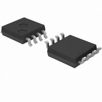
BD9850FVM-TR Rohm Semiconductor, BD9850FVM-TR Datasheet - Page 7

BD9850FVM-TR
Manufacturer Part Number
BD9850FVM-TR
Description
IC REG SW STEP DOWN HI EFF 8MSOP
Manufacturer
Rohm Semiconductor
Type
Step-Down (Buck)r
Series
-r
Datasheet
1.BD9850FVM-TR.pdf
(17 pages)
Specifications of BD9850FVM-TR
Internal Switch(s)
No
Synchronous Rectifier
No
Number Of Outputs
1
Current - Output
200mA
Frequency - Switching
100kHz ~ 2MHz
Voltage - Input
4 ~ 9 V
Operating Temperature
-40°C ~ 85°C
Mounting Type
Surface Mount
Package / Case
8-MSOP, Micro8™, 8-uMAX, 8-uSOP,
Power - Output
587mW
Mounting Style
SMD/SMT
Pwm Type
Controller
Frequency - Max
2MHz
Duty Cycle
-
Voltage - Supply
4 V ~ 9 V
Buck
Yes
Boost
No
Flyback
No
Inverting
No
Doubler
No
Divider
No
Cuk
No
Isolated
No
Lead Free Status / RoHS Status
Lead free / RoHS Compliant
Voltage - Output
-
Lead Free Status / Rohs Status
Lead free / RoHS Compliant
Available stocks
Company
Part Number
Manufacturer
Quantity
Price
Company:
Part Number:
BD9850FVM-TR
Manufacturer:
ST
Quantity:
110
Part Number:
BD9850FVM-TR
Manufacturer:
ROHM/罗姆
Quantity:
20 000
Block diagram / Pin assignment
(BD9850FVM)
(BD9851EFV)
V
REF
Vo2
Vo1
V
REF
V
REF
V
Vcc
NON2
DTC2
DTC1
REF
INV1
INV1
SCP
FB2
FB1
Vcc
RT
CT
Fig.14 BD9851EFV Block diagram
18
17
15
16
13
14
6
5
4
7
2
3
1V
–
+
–
+
OSC
Tmer
Latch
V
(2.5V)
REF
INV
FB
5
6
+
+
–
–
–
–
U.V.L.O
Both channels
1.0V
2.3V
–
ON/OFF
+
+
Error Amp
T.S.D
Vcc
V
Vcc
REF
1
Fig.13 BD9850FVM Block diagram
Pin No.
Clamper
19
12
10
11
20
1
9
8
PGND
OUT2
GND
SEL1
PVcc1
OUT1
PVcc2
1
2
3
4
5
6
7
8
STB
Vcc
V
REF
Vcc
Vcc
CTL/SS
V
4
REF
Vo1
Pin name
Vo2
CTL /SS
GND
OUT
V
Vcc
INV
FB
RT
REF
7
7/16
Pin No.
Power supply
FET driver drive output
Ground
Reference voltage (2.5V±1%) output
Error Amp inverting input
Error Amp output
Control/Soft start common
Oscillation frequency setting resistor connection
RT
PWM COMP
10
11
12
13
14
15
16
17
18
19
20
1
2
3
4
5
6
7
8
9
–
TRI
8
Pin name
reverse
FIN on
NON2
PV
PGND
PV
DTC2
OUT2
OUT1
DTC1
SEL1
INV2
INV1
GND
SCP
VR
FB2
FB1
STB
V
RT
CT
CC
CC
CC
EF
2
1
CH1 drive FET setting (Vcc short: P-ch drive, GND short: N-ch drive)
Oscillation frequency setting resistor connection
Oscillation frequency setting capacitor connection
Error Amp non-inverting input (CH2)
Error Amp inverting input (CH2)
Error Amp output (CH2)
Maximum duty/soft start setting (CH2)
FET driver block power supply input (CH2)
FET driver block output (CH2)
FET driver block ground
FET driver block output (CH1)
FET driver block power supply input (CH1)
Maximum duty/soft start setting (CH1)
Short circuit protection timer setting capacitor connection
Error Amp output (CH1)
Error Amp inverting input (CH1)
Reference voltage (2.5V±1%) output
Power supply input
ON/OFF control
Ground
Make FIN on the reverse open or ground to GND (pin 20)
(However, open FIN on the reverse will degrade radiation performance.)
GND
Function
3
Vcc
2
OUT
Function
Vcc
Vo


