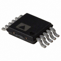
ADP1621ARMZ-R7 Analog Devices Inc, ADP1621ARMZ-R7 Datasheet - Page 13

ADP1621ARMZ-R7
Manufacturer Part Number
ADP1621ARMZ-R7
Description
IC CTRLR DC/DC PWM STEPUP 10MSOP
Manufacturer
Analog Devices Inc
Type
Step-Up (Boost)r
Datasheet
1.ADP1621ARMZ-R7.pdf
(32 pages)
Specifications of ADP1621ARMZ-R7
Internal Switch(s)
No
Synchronous Rectifier
Yes
Number Of Outputs
1
Current - Output
1A
Frequency - Switching
100kHz ~ 1.5MHz
Voltage - Input
2.9 ~ 5.5 V
Operating Temperature
-40°C ~ 125°C
Mounting Type
Surface Mount
Package / Case
10-MSOP, Micro10™, 10-uMAX, 10-uSOP
Primary Input Voltage
5.5V
No. Of Outputs
1
Output Current
1A
No. Of Pins
10
Operating Temperature Range
-40°C To +125°C
Msl
MSL 1 - Unlimited
Frequency Max
1.5MHz
Termination Type
SMD
Lead Free Status / RoHS Status
Lead free / RoHS Compliant
For Use With
ADP1621-EVALZ - BOARD EVALUATION FOR ADP1621
Voltage - Output
-
Power - Output
-
Lead Free Status / RoHS Status
Lead free / RoHS Compliant, Lead free / RoHS Compliant
Other names
ADP1621ARMZ-R7
ADP1621ARMZ-R7TR
ADP1621ARMZ-R7TR
CURRENT LIMIT
The current limit is achieved by the COMP voltage clamp, owing
to the current-mode operation of the ADP1621. A detailed
explanation of how the current limit is determined can be found
in the Current Limit section of the Application Information:
Boost Converter section.
UNDERVOLTAGE LOCKOUT
An internal undervoltage lockout (UVLO) circuit at the IN pin
holds the GATE voltage low when the IN voltage is below the
UVLO voltage, which is typically 2.5 V.
SHUTDOWN
The ADP1621 goes into shutdown approximately 50 μs after the
SDSN pin is pulled low or left floating. There is an internal 100 kΩ
resistor connected between SDSN and GND.
When the junction temperature of the ADP1621 reaches about
150°C, the ADP1621 goes into thermal shutdown and the GATE
voltage is pulled low. When the junction temperature drops below
about 140°C, the ADP1621 resumes normal operation after the
soft start sequence.
SOFT START
The ADP1621 has an internal soft start circuit that ramps
the FB regulation voltage from 0 V to 1.215 V in 64 steps over
2048 clock oscillator cycles. This soft start ramp allows the
output voltage to slowly rise to the steady-state output voltage,
preventing input inrush current at startup.
INTERNAL SHUNT REGULATORS
The IN and PIN pins each have an internal shunt regulator that
allows the ADP1621 to operate over a wide input voltage range.
The shunt regulators limit the voltages at IN and PIN to about
5.5 V, allowing the use of logic-level MOSFETs independent of
the input and/or output voltage. The shunt regulator voltage can
reach 5.7 V at 10 mA. See Figure 9 for the I-V characteristics of
these shunt regulators.
The internal power is derived from the IN pin, whereas the
MOSFET gate driver (GATE) current comes from the power
input, PIN. By separating the two inputs, PIN can be driven
with an external small-signal NPN transistor to limit the power
loss in the PIN shunt regulator when the input voltage is higher
than 5.5 V. See Figure 37 for an example. The maximum currents
going into PIN and IN should not exceed 35 mA and 25 mA,
respectively.
Rev. A | Page 13 of 32
SETTING THE OSCILLATOR FREQUENCY AND
SYNCHRONIZATION FREQUENCY
The free-running oscillator frequency, f
from FREQ to GND. A 100 kΩ resistor sets the typical oscillator
frequency to 200 kHz, a 65 kΩ resistor sets it to 325 kHz, a 32 kΩ
resistor sets it to 600 kHz, and a 10 kΩ resistor sets it to 1.5 MHz.
Figure 30 shows a typical relationship between f
The switching frequency can be synchronized to an external clock
by driving the SDSN pin with that clock signal. The SDSN pin
serves the two functions of shutdown control and frequency
synchronization input. If the SDSN input detects a low-to-high
transition within 10 μs of a high-to-low transition, it resets the
oscillator to synchronize to the frequency of the signal at SDSN.
The ADP1621 only synchronizes to frequencies greater than the
free-running switching frequency. To ensure proper synchronization
operation, set the synchronization frequency, f
running frequency, f
f
high as 1.8 MHz, the peak slope-compensation current decreases at
higher f
1.4× of f
for the synchronization frequency (see the Slope Compensation
section). For SDSN to detect a high input, the high state must
remain high for at least 100 ns.
SYNC
. Although the switching frequency can be synchronized to as
1600
1500
1400
1300
1200
1100
1000
900
800
700
600
500
400
300
200
100
SYNC
OSC
0
0
. The slope-compensation resistor, R
. It is recommended that the maximum f
20
40
OSC
. The switching frequency, f
Figure 30. f
60
80
R
FREQ
OSC
100
vs. R
(kΩ)
120
FREQ
OSC
140
, is set by a resistor
SYNC
S
, should be chosen
160
, to 1.2× the free-
OSC
SYNC
ADP1621
SW
and R
180
, is equal to
be less than
200
FREQ
.


