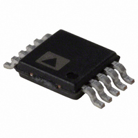
ADP1621ARMZ-R7 Analog Devices Inc, ADP1621ARMZ-R7 Datasheet - Page 20

ADP1621ARMZ-R7
Manufacturer Part Number
ADP1621ARMZ-R7
Description
IC CTRLR DC/DC PWM STEPUP 10MSOP
Manufacturer
Analog Devices Inc
Type
Step-Up (Boost)r
Datasheet
1.ADP1621ARMZ-R7.pdf
(32 pages)
Specifications of ADP1621ARMZ-R7
Internal Switch(s)
No
Synchronous Rectifier
Yes
Number Of Outputs
1
Current - Output
1A
Frequency - Switching
100kHz ~ 1.5MHz
Voltage - Input
2.9 ~ 5.5 V
Operating Temperature
-40°C ~ 125°C
Mounting Type
Surface Mount
Package / Case
10-MSOP, Micro10™, 10-uMAX, 10-uSOP
Primary Input Voltage
5.5V
No. Of Outputs
1
Output Current
1A
No. Of Pins
10
Operating Temperature Range
-40°C To +125°C
Msl
MSL 1 - Unlimited
Frequency Max
1.5MHz
Termination Type
SMD
Lead Free Status / RoHS Status
Lead free / RoHS Compliant
For Use With
ADP1621-EVALZ - BOARD EVALUATION FOR ADP1621
Voltage - Output
-
Power - Output
-
Lead Free Status / RoHS Status
Lead free / RoHS Compliant, Lead free / RoHS Compliant
Other names
ADP1621ARMZ-R7
ADP1621ARMZ-R7TR
ADP1621ARMZ-R7TR
ADP1621
LAYOUT CONSIDERATIONS
Layout is important for all switching regulators, but is par-
ticularly important for regulators with high switching frequencies.
To achieve high efficiency, good regulation, and stability, a well-
designed printed circuit board layout is required. A sample PCB
layout for the standard boost converter circuit shown in Figure 33
is given in Figure 32.
Follow these guidelines when designing printed circuit boards:
•
•
•
•
•
Keep the low ESR bypass input capacitor of 0.1 μF or higher
close to IN/PIN and GND.
Keep the high current path from Bulk Input Capacitor C1
through Inductor L1 and MOSFET M1 to PGND as short
as possible.
Keep the high current path from Bulk Input Capacitor C1
through Inductor L1, Diode D1, and Output Capacitor C
to PGND as short as possible. Place C
as possible to reduce ground bouncing.
Keep high current traces as short and wide as possible to
minimize parasitic series inductance, which causes spiking
and electromagnetic interference (EMI).
To minimize switching noise, the drain of the power MOSFET
should be placed very close to the inductor, and the source
of the MOSFET (or the bottom side of the sense resistor)
should be connected directly to the power GND plane. Use
wide copper traces on the drain and on the source of the
MOSFET to minimize parasitic inductance and resistance.
Parasitic inductance can lead to excessive ringing during
switching transitions, and parasitic resistance reduces the
converter efficiency. Make sure that the MOSFET selected
is capable of handling the total power loss (conduction plus
transition losses) in the application circuit.
Figure 32. PCB Layout of the Circuit Shown in Figure 33 (2-layer PCB)
OUT
VIAS TO GND PLANE
VIAS TO 2ND LAYER
as close to PGND
L1
SDSN
V
IN
OUT
Rev. A | Page 20 of 32
GND
ADP1621
M1
C1
R
GATE
FREQ
D1
GND
•
•
•
•
•
•
•
•
REMOTE OUTPUT
Avoid routing high impedance traces near any node con-
nected to the switch node (the MOSFET drain) or near
Inductor L1 to prevent radiated switching-noise injection.
Add an extra copper plane at the connection of the MOSFET
drain and the anode of the diode to help dissipate the heat
generated by losses in those components.
Avoid ground loops by having one central ground node on the
PCB. If this is impractical, place the power ground with high
current levels physically closer to the PCB ground terminal.
The analog, low current-level ground should be placed farther
from the PCB ground terminal.
Minimize the length of the PCB trace between the GATE
pin and the MOSFET gate. The parasitic inductance in this
PCB trace can give rise to excessive voltage ringing at the
MOSFET gate and drain, as well as the regulator output. It
is recommended to add 5 Ω of resistance for every inch of
PCB trace. This helps to reduce the overshoot and ringing at
the drain and the output. However, this added resistance
increases the rise and fall times of the MOSFET; thus, the
switching loss in the MOSFET is increased.
Place the feedback resistors as close to FB as possible to
prevent high frequency switching-noise injection.
Place the top of the upper feedback resistor, R1, as close
as possible to the top of C
sensing.
If a current-sense resistor is connected between the source
of the MOSFET and PGND, ensure that the capacitance from
CS to PGND is minimized.
Place the compensation components as close as possible
to COMP.
SENSING
C
C
C
OUT1
OUT2
OUT3
V
OUT
OUT
for optimum output voltage


