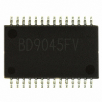
BD9045FV-E2 Rohm Semiconductor, BD9045FV-E2 Datasheet

BD9045FV-E2
Specifications of BD9045FV-E2
Available stocks
Related parts for BD9045FV-E2
BD9045FV-E2 Summary of contents
Page 1
... BD9040FV, BD9045FV ●Outline BD9040FV and BD9045FV are 1ch, and 2ch switching controllers that can be used within the wide range of the input. Highly effective can be achieved by the synchronous rectification method and it is possible to contribute to the eco-design of all electronic equipment (energy-saving). ...
Page 2
Electric characteristic ( as long as it doesn't specify it Ta=25℃ VCC=12V EN=5V) (BD9040FV) Item VCC Current of bias Standby current [VREG5] Standard voltage output voltage Load stability level [VREG3 part] Standard voltage Load stability level [prevention part for ...
Page 3
... AMBIENT TEMPERATURE : Ta[ ℃ ] Fig.6 Frequency temperature characteristic 3.5 3.0 2.5 2.0 1.5 1.0 0.5 0 INPUT VOLTAGE : V Fig9. EN Threshold voltage V OUT I OUT Fig.12 Load response 2 BD9045FV BD9040FV ℃ 25 ℃ -40 ℃ [V] EN 20mV/div 1A/div ...
Page 4
BD9040FV ○ Pin distribution chart 1 EN_SS COMP N.C. 9 VREG3 GND 10 ○Block chart VREG5 3.8V ○Terminal number and terminal name Terminal number BOOT ...
Page 5
... BD9045FV ○Pin distribution chart 15 14 GND 13 16 TM1 12 17 SS1 18 11 COMP1 10 19 FB1 EN1 VCC 22 7 EN2 23 6 VREG3 FB2 26 3 COMP2 27 2 SS2 28 1 TM2 ○Block chart 5V Reg VREG5 3.8V TM2 CL2 BOOT2 OUTH2 SW2 VREG5 OUTL2 DGND2 FB2 - ...
Page 6
... At the time of EN=L, the capacitors of OFF, TM and SS of output are discharged, and become the standby state. (As for BD9045FV, due to EN1 and EN2, the capacitors of OFF, TM and SS of each ch output are discharged. In addition it becomes the standby state when both EN1 and EN2 are made to be L). ...
Page 7
... COMP 3kΩ 47pF FB EN N.C. VREG3 0.1uF GND These characteristics vary with the layout of board and the kind of parts etc, so please confirm them thoroughly with actual devices. BD9045FV 0.1uF 10nF 0.1uF 3.3kΩ 22pF 0.1uF 82kΩ 10nF 100pF 2kΩ 0.1uF ...
Page 8
Method to select the application parts (1) Setting of output L constant Δ IL VCC I L VOUT L Co Output ripple current If a current exceeding the rated current value of coil flows in coil, the coil will ...
Page 9
Design of feedback resistance constant Please refer to the following formula for design of feedback resistance. The 1kΩ~330kΩ is recommended as its setting range more than 1kΩ, drop in electric power efficiency will be caused. ...
Page 10
... This OFF latch is released once EN is made to be「 L 」or if VCC is once lowered and then rises again [kΩ] CL VCC ΔVsw OUTH Io SW OUTL [sec] ・・・ (10) 10/16 In case of SP8K2 BD9045FV measurement value of our company’s substrate Compare the V that is set generated by ON resistance of loxFET. and the ΔVsw that ...
Page 11
Method to set the phase compensation ・Stable condition of application Shown as below are the stable conditions of the feedback system for negative feedback to return. ・The phase delay when the gain is 1(0dB more than150°(i.e. phase ...
Page 12
OS CON etc, ESR of which is small If an output capacitor, ESR of which is small (a few mΩ), is used in the output necessary to insert two different phase ...
Page 13
Timing chart VCC SS EN1 Vreg3 Vreg5 TM FB EN=L EN=L 1V 1.1V OVP 検出 0.45V OVP detection SCP detection SCP 検出 on latch condition ラッチ状態で output OFF 出力 OFF 13/16 EN=L UVLO 4.2V 3. latch condition ...
Page 14
... VCC 300kΩ EN_SS 200kΩ 100kΩ 9PIN [VREG3] (23)PIN [VREG3] VCC 2kΩ VREG3 50Ω 14/16 The inside BD9045FV (20,22)PIN [EN1, EN2] VCC VCC 377kΩ EN 315kΩ 184kΩ 5PIN [COMP] (18,26)PIN [COMP1, COMP2] VREG3 VREG5 20kΩ COMP ...
Page 15
Absolute maximum specification If absolute maximum rating such as applied voltage and working temperature range etc. is exceeded, deterioration or breakdown may occur as a result. Moreover, such destructive conditions as short mode or open mode etc. can not ...
Page 16
GND recommended to carry out the one-point grounding at the reference point of set. Please be careful of not changing the GND wiring pattern of external parts. 13. SW terminal In case of connecting of application, SW ...
Page 17
Appendix No technical content pages of this document may be reproduced in any form or transmitted by any means without prior permission of ROHM CO.,LTD. The contents described herein are subject to change without notice. The specifications for the product ...


