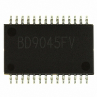
BD9045FV-E2 Rohm Semiconductor, BD9045FV-E2 Datasheet - Page 6

BD9045FV-E2
Manufacturer Part Number
BD9045FV-E2
Description
IC REG SW STEP DOWN HE 28SSOP
Manufacturer
Rohm Semiconductor
Type
Step-Down (Buck)r
Datasheet
1.BD9040FV-E2.pdf
(17 pages)
Specifications of BD9045FV-E2
Internal Switch(s)
No
Synchronous Rectifier
Yes
Number Of Outputs
2
Frequency - Switching
200kHz ~ 750kHz
Voltage - Input
4.5 ~ 18 V
Mounting Type
Surface Mount
Package / Case
28-SSOP
Power - Output
940mW
Primary Input Voltage
12V
No. Of Outputs
1
Output Voltage
5.5V
Output Current
6mA
Voltage Regulator Case Style
SSOP
No. Of Pins
28
Operating Temperature Range
-40°C To +85°C
Svhc
No SVHC
Lead Free Status / RoHS Status
Lead free / RoHS Compliant
Current - Output
-
Voltage - Output
-
Operating Temperature
-
Lead Free Status / Rohs Status
Lead free / RoHS Compliant
Other names
BD9045FV-E2TR
Available stocks
Company
Part Number
Manufacturer
Quantity
Price
Company:
Part Number:
BD9045FV-E2
Manufacturer:
ROHM
Quantity:
2 448
○ Operational description of each block
・Error amplifier(ErrAmp)
・Oscillator(OSC)
・SLOPE
・PWM Comparator(PWM COMP)
・Reference voltage(5V Reg, 3V Reg)
・Overcurrent protection circuit(OCP)
・Overvoltage protection circuit(OVP)
・Output short circuit protection circuit
・O/S Check
・Under Voltage Lockout (UVLO) / Thermal Shutdown(TSD)
・Function of EN
・Function of EN_SS(BD9040FV alone)
It is a circuit to compare the 0.9V reference voltage and the output voltage’s feedback voltage. Switching Duty is determined
by the COMP voltage that is the result of the comparison. In addition, due to the SS terminal voltage on start-up, the Soft
Start begins operating, and so the COMP voltage is limited by the SS voltage.
It is a block, the oscillating frequency of which is decided by RT and can be set up to 200kHz~750kHz.
It is a block in which triangular wave is created from the clock generated by the OSC. And the generated triangular wave is
transmitted to the PWM comparator.
The error amplifier’s output COMP voltage and the SLOPE block’s triangular wave are compared, and the switching Duty is
determined. The switching duty is limited by the maximum Duty ratio internally decided and can not become 100%.
It is a block to generate 5.5V and 3V internal reference voltage.
At the time of OUTH=H, if SW voltage becomes not more than CL voltage, the overcurrent protection circuit operates. When
the overcurrent protection operates, the Duty is limited, and so the output voltage is lowered. Moreover, when an overcurrent
is detected by the overcurrent protection circuit, the charging of the external capacitor on TM terminal is started. When the
voltage on TM terminal exceeds 1V, the output becomes OFF state and then is latched. Once EN is made to be L, the latch is
released.
When FB voltage becomes more than 1.1 V, the overvoltage protection operates. When the overvoltage protection operates,
the charging of the external capacitor on TM terminal is started. When the voltage on TM terminal exceeds 1V, the output
becomes OFF state and then is latched. Once EN is made to be L, the latch is released.
If FB voltage becomes not more than 0.4V, the output short circuit protection circuit operates. When the output short circuit
protection operates, the charging of the external capacitor on TM terminal is started. When the voltage on TM terminal
exceeds 1V, the output becomes OFF state and then is latched. Once EN is made to be L, the latch is released.
When RT terminals become open or short circuit states, RT OPEN and SHORT circuit protections operate respectively.
When RT terminals’ open or short circuit state is detected, the charging of the external capacitor on TM terminal is started.
When the voltage on TM terminal exceeds 1V, the output becomes OFF state and then is latched. Once EN is made to be L,
the latch is released.
When VREG5 becomes no more than around 3.8V or VREG3 no more than around 2.5, the output of the under voltage
lockout is turned off.
Then, When VREG5 becomes more than around 4.2V or VREG3 more than around 2.6, the output of the under voltage
lockout is reset.
Moreover, when the temperature of chip becomes more than around 150 , the output of the thermal shutdown (TSD) is
turned off, and when it is returned to a certain temperature, the output is reset.
When UVLO and TSD operate, the capacitors of TM and SS are discharged.
EN is pulled down in regard to GND and pulled up in regard to VCC, and normally EN=H.
At the time of EN=L, the capacitors of OFF, TM and SS of output are discharged, and become the standby state.
(As for BD9045FV, due to EN1 and EN2, the capacitors of OFF, TM and SS of each ch output are discharged. In addition it
becomes the standby state when both EN1 and EN2 are made to be L).
EN_SS is pulled down in regard to GND and pulled up in regard to VCC, and normally EN_SS=H.
At the time of EN_SS=L, the capacitors of OFF, TM and SS of output are discharged.
At the time of EN_SS=L, the capacitor of SS is constant-current discharged, so it can be made delayed during output’s OFF.
6/16


