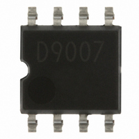
BD9007F-E2 Rohm Semiconductor, BD9007F-E2 Datasheet - Page 8

BD9007F-E2
Manufacturer Part Number
BD9007F-E2
Description
IC REG SW 2A FLEX STEPDOWN 8-SOP
Manufacturer
Rohm Semiconductor
Type
Step-Down (Buck)r
Datasheet
1.BD9006F-E2.pdf
(18 pages)
Specifications of BD9007F-E2
Internal Switch(s)
Yes
Synchronous Rectifier
No
Number Of Outputs
1
Voltage - Output
1 ~ 35 V
Current - Output
2A
Frequency - Switching
50kHz ~ 500kHz
Voltage - Input
7 ~ 35 V
Operating Temperature
-40°C ~ 105°C
Mounting Type
Surface Mount
Package / Case
8-SOP
Power - Output
690mW
Output Voltage
2. 6 V
Output Current
2 A
Input Voltage
7 V to 35 V
Operating Temperature Range
- 40 C to + 105 C
Mounting Style
SMD/SMT
Duty Cycle (max)
100 %
Lead Free Status / RoHS Status
Lead free / RoHS Compliant
Other names
BD9007F-E2TR
●Description of operations
BD9006F, BD9006HFP, BD9007F, BD9007HFP
© 2009 ROHM Co., Ltd. All rights reserved.
www.rohm.com
・ERROR AMP
・SOFT START
・SYNC
・OSC(Oscillator)
・slope
・PWM COMPARATOR
・TSD (Thermal Shut Down)
・CURRENT LIMIT
The ERROR AMP block is an error amplifier used to input the reference voltage (0.8V Typ.) and the INV pin voltage. The
output FB pin controls the switching duty and output voltage Vo. These INV and FB pins are externally mounted to
facilitate phase compensation. Inserting a capacitor and resistor between these pins enables adjustment of phase margin.
(Refer to recommended examples on pages 11~13.)
The SOFT START block provides a function to prevent the overshoot of the output voltage Vo through gradually
increasing the normal rotation input of the error amplifier when power supply turns ON to gradually increase the switching
Duty. The soft start time is set to 5msec (Typ.).
By making the “EN/SYNC” terminal less than 0.8V, the circuit can be shut down.
Furthermore, by applying pulse with higher frequency than the configured oscillation frequency to the “EN/SYNC”
terminal, external sync is possible. (Sync possible with double the configured frequency-configured frequency or 500kHz)
This circuit generates the pulse wave to be input to the slope, and by connecting resistance to “RT”, 50~500kHz
oscillating frequency can be configured. (Refer to p.11 Fig.24)
This block generates saw tooth waves from the clock generated by the OSC. The generated saw tooth waves are sent
to PWM COMPARATOR.
The PWM COMPARATOR block is a comparator to make comparison between the FB pin and internal saw tooth wave
and output a switching pulse
The switching pulse duty varies with the FB value. (min Duty width : 250ns.)
In order to prevent thermal destruction/thermal runaway of the IC, the TSD block will turn OFF the output when the chip
temperature reaches approximately 150℃ or more. When the chip temperature falls to a specified level, the output will be
reset. However, since the TSD is designed to protect the IC, the chip junction temperature should be provided with the
thermal shutdown detection temperature of less than approximately.150℃.
While the output POWER P-ch MOS FET is ON, if the voltage between drain and source (ON resistance×load current)
exceeds the reference voltage internally set with the IC, this block will turn OFF the output to latch. The overcurrent
protection detection values have been set as shown below:
Furthermore, since this overcurrent protection is an automatically reset, after the output is turned OFF and latched, the
latch will be reset with the RESET signal output by each oscillation frequency.
However, this protection circuit is only effective in preventing destruction from sudden accident. It does not support for the
continuous operation of the protection circuit (e.g. if a load, which significantly exceeds the output current capacitance, is
normally connected). Furthermore, since the overcurrent protection detection value has negative temperature
characteristics, consider thermal design.
BD9006F,BD9006HFP, BD9007F,BD9007HFP ・・・ 4A (Typ.)
8/17
Technical Note
2009.05 - Rev.A


