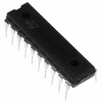
L4972A STMicroelectronics, L4972A Datasheet - Page 3

L4972A
Manufacturer Part Number
L4972A
Description
IC REG SW 2A 5.1V-40V 20-DIP
Manufacturer
STMicroelectronics
Type
Step-Down (Buck)r
Datasheet
1.L4972AD013TR.pdf
(22 pages)
Specifications of L4972A
Internal Switch(s)
Yes
Synchronous Rectifier
No
Number Of Outputs
1
Voltage - Output
5.1 ~ 40 V
Current - Output
2A
Frequency - Switching
100kHz
Voltage - Input
15 ~ 50 V
Operating Temperature
-40°C ~ 150°C
Mounting Type
Through Hole
Package / Case
20-DIP (0.300", 7.62mm)
Power - Output
5W
Output Voltage
50 V
Mounting Style
Through Hole
Input Voltage
50V
Output Current
2A
No. Of Outputs
1
Power Dissipation Pd
5W
No. Of Pins
20
Operating Temperature Range
-40°C To +150°C
Filter Terminals
Through Hole
Rohs Compliant
Yes
Lead Free Status / RoHS Status
Lead free / RoHS Compliant
Other names
497-6698-5
L4972A
L4972A
Available stocks
Company
Part Number
Manufacturer
Quantity
Price
Part Number:
L4972A
Manufacturer:
ST
Quantity:
20 000
Company:
Part Number:
L4972AD
Manufacturer:
STM
Quantity:
3 697
Part Number:
L4972AD
Manufacturer:
STM
Quantity:
20 000
Company:
Part Number:
L4972AD013TR
Manufacturer:
SII
Quantity:
4 466
Part Number:
L4972AD013TR
Manufacturer:
ST
Quantity:
20 000
Table 3. Absolute Maximum Ratings
(*) SO-20
Table 4. Thermal Data
3
The L4972A is a 2A monolithic stepdown switching regulator working in continuous mode realized in the
new BCD Technology. This technology allows the integration of isolated vertical DMOS power transistors
plus mixed CMOS/Bipolar transistors.
The device can deliver 2A at an output voltage adjustable from 5.1V to 40V and contains diagnostic and
control functions that make it particularly suitable for microprocessor based systems.
3.1 BLOCK DIAGRAM
The block diagram shows the DMOS power transistors and the PWM control loop. Integrated functions
include a reference voltage trimmed to 5.1V ± 2%, soft start, undervoltage lockout, oscillator with feedfor-
ward control, pulse by pulse current limit, thermal shutdown and finally the reset and power fail circuit. The
reset and power fail circuit provides an output signal for a microprocessor indicating the status of the sys-
tem.
Device turn on is around 11V with a typical 1V hysterysis, this threshold porvides a correct voltage for the
driving stage of the DMOS gate and the hysterysis prevents instabilities.
An external bootstrap capacitor charge to 12V by an internal voltage reference is needed to provide cor-
rect gate drive to the power DMOS. The driving circuit is able to source and sink peak currents of around
0.5A to the gate of the DMOS transistor. A typical switching time of the current in the DMOS transistor is
50ns. Due to the fast commutation switching frequencies up to 200kHz are possible.
The PWM control loop consists of a sawtooth oscillator, error amplifier, comparator, latch and the output
V
Symbol
Symbol
R
R
2
T
V
, V
th j-amb
J
th j-pins
V
V
V
V
P
4
I
, T
V
Circuit Operation
V
I
I
I
I
20
, V
11
11
20
10
tot
3
2
7
8
7
3
I
, V
stg
8
9
,
Input Voltage
Input Operating Voltage
Output DC Voltage
Output Peak Voltage at t = 0.1µs f = 200kHz
Maximum Output Current
Boostrap Voltage
Boostrap Operating Voltage
Input Voltage at Pins 4, 12
Reset Output Voltage
Reset Output Sink Current
Input Voltage at Pin 2, 7, 9, 10
Reset Delay Sink Current
Error Amplifier Output Sink Current
Soft Start Sink Current
Total Power Dissipation at T
Junction and Storage Temperature
Thermal Resistance Junction-Pins
Thermal Resistance Junction-ambient
at Tamb = 70°C (No copper area on PCB)
Parameter
Parameter
PINS
≤ 90°C
max,
max,
PowerDIP
Internally Limited
12
60
-40 to 150
5 / 3.75(*)
V
1.3/1 (*)
Value
11
55
50
65
12
50
50
30
30
-1
-5
7
1
+ 15
SO20
16
80
L4972A
°C/W
°C/W
Unit
Unit
mA
mA
mA
°C
W
W
V
V
V
V
V
V
V
V
A
V
3/22


