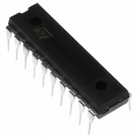
L4972A STMicroelectronics, L4972A Datasheet - Page 7

L4972A
Manufacturer Part Number
L4972A
Description
IC REG SW 2A 5.1V-40V 20-DIP
Manufacturer
STMicroelectronics
Type
Step-Down (Buck)r
Datasheet
1.L4972AD013TR.pdf
(22 pages)
Specifications of L4972A
Internal Switch(s)
Yes
Synchronous Rectifier
No
Number Of Outputs
1
Voltage - Output
5.1 ~ 40 V
Current - Output
2A
Frequency - Switching
100kHz
Voltage - Input
15 ~ 50 V
Operating Temperature
-40°C ~ 150°C
Mounting Type
Through Hole
Package / Case
20-DIP (0.300", 7.62mm)
Power - Output
5W
Output Voltage
50 V
Mounting Style
Through Hole
Input Voltage
50V
Output Current
2A
No. Of Outputs
1
Power Dissipation Pd
5W
No. Of Pins
20
Operating Temperature Range
-40°C To +150°C
Filter Terminals
Through Hole
Rohs Compliant
Yes
Lead Free Status / RoHS Status
Lead free / RoHS Compliant
Other names
497-6698-5
L4972A
L4972A
Available stocks
Company
Part Number
Manufacturer
Quantity
Price
Part Number:
L4972A
Manufacturer:
ST
Quantity:
20 000
Company:
Part Number:
L4972AD
Manufacturer:
STM
Quantity:
3 697
Part Number:
L4972AD
Manufacturer:
STM
Quantity:
20 000
Company:
Part Number:
L4972AD013TR
Manufacturer:
SII
Quantity:
4 466
Part Number:
L4972AD013TR
Manufacturer:
ST
Quantity:
20 000
Table 5. Electrical Characteristcs (continued)
Refer to the test circuit, T
specified.
SOFT START (pin 8)
ERROR AMPLIFIER
RAMP GENERATOR (pin 18)
SYNC FUNCTION (pin 10)
RESET AND POWER FAIL FUNCTIONS
Symbol
SVR
V
I
V
I
V
V
I
V
V
V
V
V
I
V
V
V
V
-I
I
G
I
2SO
V
I
I
10H
20L
10L
t
2SI
I
7H
I
I
18
18
OS
7H
7L
W
9R
9F
2H
3S
8
7L
9
18
18
10
10
10
2L
3
8
V
Out Leak Current
Soft Start Source Current
Output Saturation Voltage
High Level Out Voltage
Low Level Out Voltage
Source Output Current
Sink Output Current
Input Bias Current
DC Open Loop Gain
Supply Voltage Rejection
Input Offset Voltage
Ramp Valley
Ramp Peak
Min. Ramp Current
Max. Ramp Current
Low Input Voltage
High Input voltage
Sync Input Current with Low
Input Voltage
Input Current with High
Input Voltage
Output Amplitude
Output Pulse Width
Rising Thereshold Voltage (pin 9) V
Falling Thereshold Voltage (pin 9) V
Delay High Threshold Volt.
Delay Low Threshold Volt.
Delay Source Current
Delay Source Sink Current
Output Saturation Voltage
Output Leak Current
Parameter
J
= 25°C, V
i
= 35V, R4 = 30KΩ, C9 = 2.7nF, f
V
V
V
R
S1 = A; I
V
V
I
I
I
I
S1 = B; R
S1 = A; R
15 < V
S1 = B; S2 = B
S1 = B; S2 = B
V
V
S1 = A; I
V
S1 = B; S2 = B; S4 = B
V
V
S1 = B; S2 = B
V
V
V
V
V
V
V
V
I
V
8
8
7
7
3
i
i
8
= 200µA; V
7
7
i
i
i
8
10
10
thr
i
4
i
4
i
4
4
4
3
S
= 100µA; S1 = C; V
= 20mA; V
= 100µA; S1 = C; V
= 15mA; S1 = B V
= 15 to 50V;V
= 55V; S3 = A; V
= 15V
= 45V
= 15V to 50V; V
= 15 to 50V
= 15 to 50V
= 15 to 50V
= 50Ω S1 = A
= 3V; V
= 1V; V
= 6V; V
= 0; S1 = B; S2 = B; S4 = B
= 5.3V
= 5.3V
= 5.3V; V
= 5.3V; V
= 4.7V; V
= 50V; S1 = A
= V
= 2.5V
= 2.5V
i
18
< 50V
Test Condition
17
17
= 0.9V; S4 = B;
S
S
9
7
9
= 100µA
= 1mA
= 10Ω
= 0V
= 10KΩ
= 4.7V
= 5.3V
9
2
2
11
11
= V
= 3V
= 3V
= 10V
= 10V
4
= 4.7V; V
13
8
8
= 0;
= 0
4
9
9
= 4.7V
= 5.3V
= 4.7V
9
= V
13
Min.
–0.3
-130
4.77
4.95
100
100
V
1.2
2.4
2.5
0.3
80
60
60
30
10
SW
6
4
1
ref
= 100KHz typ, unless otherwise
Typ.
-100
-200
115
150
150
270
V
V
0.4
1.5
2.5
5.5
2.7
0.5
5.1
1.1
80
60
2
5
ref
ref
Max.
-160
5.25
150
300
100
V
V
0.7
0.9
5.5
0.4
1.5
-80
0.4
1.2
0.8
1.2
10
80
2
1
3
ref
ref
Unit
mA
mV
mA
mA
mA
mV
mV
mA
µA
µA
µA
µA
dB
dB
µA
µA
µA
µs
V
V
V
V
V
V
V
V
V
V
V
V
V
V
V
L4972A
Fig.
12
13
13
13
14
14
14
14
14
14
14
14
12
12
12
12
12
12
12
12
12
15
15
15
15
15
15
15
15
7/22
–
–


