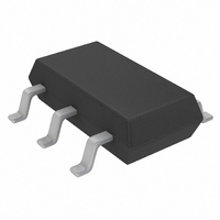
LTC1772BES6#TRM Linear Technology, LTC1772BES6#TRM Datasheet - Page 11

LTC1772BES6#TRM
Manufacturer Part Number
LTC1772BES6#TRM
Description
IC CTRLR DC/DC S-DWN SOT23-6
Manufacturer
Linear Technology
Type
Step-Down (Buck)r
Datasheet
1.LTC1772BES6TRMPBF.pdf
(16 pages)
Specifications of LTC1772BES6#TRM
Internal Switch(s)
No
Synchronous Rectifier
No
Number Of Outputs
1
Voltage - Output
0.8 ~ 9.8 V
Current - Output
1A
Frequency - Switching
550kHz
Voltage - Input
2.5 ~ 9.8 V
Operating Temperature
-40°C ~ 85°C
Mounting Type
Surface Mount
Package / Case
TSOT-23-6, TSOT-6
Lead Free Status / RoHS Status
Contains lead / RoHS non-compliant
Power - Output
-
Other names
LTC1772BES6#TRMTR
Available stocks
Company
Part Number
Manufacturer
Quantity
Price
APPLICATIONS INFORMATION
current, 2) MOSFET gate charge current, 3) I
and 4) voltage drop of the output diode.
1. The V
2. MOSFET gate charge current results from switching
3. I
4. The output diode is a major source of power loss at
electrical characteristics, that excludes MOSFET driver
and control currents. V
which increases with V
the gate capacitance of the power MOSFET. Each time a
MOSFET gate is switched from low to high to low again,
a packet of charge dQ moves from V
resulting dQ/dt is a current out of V
much larger than the DC supply current. In continuous
mode, I
the MOSFET, inductor and current shunt. In continu-
ous mode the average output current fl ows through L
but is “chopped” between the P-channel MOSFET (in
series with R
R
summed with the resistances of L and R
I
high currents and gets worse at high input voltages.
The diode loss is calculated by multiplying the forward
voltage times the diode duty cycle multiplied by the
2
2
DS(ON)
R losses are predicted from the DC resistances of
R losses.
IN
GATECHG
current is the DC supply current, given in the
plus R
SENSE)
SENSE
= f(Qp).
and the output diode. The MOSFET
multiplied by duty cycle can be
IN
IN
current results in a small loss
.
IN
IN
which is typically
to ground. The
SENSE
Figure 6. Foldback Current Limiting
2
I
TH
R losses
LTC1772B
to obtain
/RUN
V
FB
R2
R1
5. Transition losses apply to the external MOSFET and
Other losses including C
and inductor core losses, generally account for less than
2% total additional loss.
Foldback Current Limiting
As described in the Output Diode Selection, the worst-case
dissipation occurs with a short-circuited output when the
diode conducts the current limit value almost continuously.
To prevent excessive heating in the diode, foldback current
limiting can be added to reduce the current in proportion
to the severity of the fault.
Foldback current limiting is implemented by adding diodes
D
shown in Figure 6. In a hard short (V
will be reduced to approximately 50% of the maximum
output current.
FB1
+
load current. For example, assuming a duty cycle of
50% with a Schottky diode forward voltage drop of
0.4V, the loss increases from 0.5% to 8% as the load
current increases from 0.5A to 2A.
increase at higher operating frequencies and input
voltages. Transition losses can be estimated from:
Transition Loss = 2(V
and D
FB2
1772 F05
D
D
FB1
FB2
between the output and the I
V
OUT
IN
IN
and C
)
2
I
O(MAX)
OUT
ESR dissipative losses,
OUT
C
LTC1772B
RSS
= 0V), the current
(f)
TH
/RUN pin as
11
1772bfa


