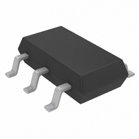
LTC1772BES6#TRM Linear Technology, LTC1772BES6#TRM Datasheet - Page 12

LTC1772BES6#TRM
Manufacturer Part Number
LTC1772BES6#TRM
Description
IC CTRLR DC/DC S-DWN SOT23-6
Manufacturer
Linear Technology
Type
Step-Down (Buck)r
Datasheet
1.LTC1772BES6TRMPBF.pdf
(16 pages)
Specifications of LTC1772BES6#TRM
Internal Switch(s)
No
Synchronous Rectifier
No
Number Of Outputs
1
Voltage - Output
0.8 ~ 9.8 V
Current - Output
1A
Frequency - Switching
550kHz
Voltage - Input
2.5 ~ 9.8 V
Operating Temperature
-40°C ~ 85°C
Mounting Type
Surface Mount
Package / Case
TSOT-23-6, TSOT-6
Lead Free Status / RoHS Status
Contains lead / RoHS non-compliant
Power - Output
-
Other names
LTC1772BES6#TRMTR
Available stocks
Company
Part Number
Manufacturer
Quantity
Price
LTC1772B
APPLICATIONS INFORMATION
PC Board Layout Checklist
When laying out the printed circuit board, the following
checklist should be used to ensure proper operation of
the LTC1772B. These items are illustrated graphically in
the layout diagram in Figure 7. Check the following in
your layout:
1. Is the Schottky diode closely connected between ground
2. Does the (+) plate of C
3. Is the input decoupling capacitor (0.1μF) connected
12
(Pin 2) and drain of the external MOSFET?
as closely as possible? This capacitor provides AC
current to the MOSFET.
closely between V
C
R
ITH
IN
ITH
(Pin 5) and ground (Pin 2)?
IN
connect to the sense resistor
Figure 7. LTC1772B Layout Diagram (See PC Board Layout Checklist)
BOLD LINES INDICATE HIGH CURRENT PATHS
1
2
3
I
GND
V
TH
FB
/RUN
LTC1772B
SENSE
PGATE
V
IN
–
6
5
4
R
0.1μF
SENSE
4. Connect the end of R
5. Is the trace from SENSE
6. Keep the switching node PGATE away from sensitive
7. Does the V
possible. The V
comparator.
kept short? Does the trace connect close to R
small signal nodes.
resistors? The resistive divider R1 and R2 must be
connected between the (+) plate of C
ground.
M1
+
C
IN
D1
FB
L1
pin connect directly to the feedback
IN
R1
+
1772 F06
pin is the SENSE
SENSE
C
OUT
–
R2
(Pin 4) to the Sense resistor
as close to V
V
V
IN
OUT
+
OUT
of the current
IN
and signal
(Pin 5) as
SENSE
1772bfa
?


