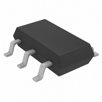
LTC1772BES6#TRM Linear Technology, LTC1772BES6#TRM Datasheet - Page 9

LTC1772BES6#TRM
Manufacturer Part Number
LTC1772BES6#TRM
Description
IC CTRLR DC/DC S-DWN SOT23-6
Manufacturer
Linear Technology
Type
Step-Down (Buck)r
Datasheet
1.LTC1772BES6TRMPBF.pdf
(16 pages)
Specifications of LTC1772BES6#TRM
Internal Switch(s)
No
Synchronous Rectifier
No
Number Of Outputs
1
Voltage - Output
0.8 ~ 9.8 V
Current - Output
1A
Frequency - Switching
550kHz
Voltage - Input
2.5 ~ 9.8 V
Operating Temperature
-40°C ~ 85°C
Mounting Type
Surface Mount
Package / Case
TSOT-23-6, TSOT-6
Lead Free Status / RoHS Status
Contains lead / RoHS non-compliant
Power - Output
-
Other names
LTC1772BES6#TRMTR
Available stocks
Company
Part Number
Manufacturer
Quantity
Price
APPLICATIONS INFORMATION
Since the LTC1772B is designed for operation down to low
input voltages, a logic level threshold MOSFET (R
guaranteed at V
work close to this voltage. When these MOSFETs are used,
make sure that the input supply to the LTC1772B is less
than the absolute maximum V
The required minimum R
by its allowable power dissipation. For applications that
may operate the LTC1772B in dropout, i.e., 100% duty
cycle, at its worst case the required R
where P
temperature dependency of R
given for a MOSFET in the form of a normalized R
vs temperature curve, but δp = 0.005/°C can be used as
an approximation for low voltage MOSFETs.
In applications where the maximum duty cycle is less
than 100% and the LTC1772B is in continuous mode, the
R
where DC is the maximum operating duty cycle of the
LTC1772B.
Output Diode Selection
The catch diode carries load current during the off-time.
The average diode current is therefore dependent on the
P-channel switch duty cycle. At high input voltages the
diode conducts most of the time. As V
the diode conducts only a small fraction of the time. The
most stressful condition for the diode is when the output
is short-circuited. Under this condition the diode must
safely handle I
it is important to adequately specify the diode peak cur-
rent and average power dissipation so as not to exceed
the diode ratings.
DS(ON)
R
R
DS(ON)
DS(ON)
P
is governed by:
is the allowable power dissipation and δp is the
DC=100%
( )
DC
PEAK
GS
= 2.5V) is required for applications that
I
=
at close to 100% duty cycle. Therefore,
OUT
(
P
I
OUT(MAX)
P
2
DS(ON)
(
1+ p
P
DS(ON)
GS
of the MOSFET is governed
P
)
)
2
rating, typically 8V.
(
1+ p
. (1 + δp) is generally
IN
DS(ON)
approaches V
)
is given by:
DS(ON)
DS(ON)
OUT
Under normal load conditions, the average current con-
ducted by the diode is:
The allowable forward voltage drop in the diode is calculated
from the maximum short-circuit current as:
where P
determined by effi ciency and/or thermal requirements.
A fast switching diode must also be used to optimize
effi ciency. Schottky diodes are a good choice for low
forward drop and fast switching times. Remember to
keep lead length short and observe proper grounding (see
Board Layout Checklist) to avoid ringing and increased
dissipation.
C
In continuous mode, the source current of the P-chan-
nel MOSFET is a square wave of duty cycle (V
(V
ESR input capacitor sized for the maximum RMS current
must be used. The maximum RMS capacitor current is
given by:
This formula has a maximum value at V
I
monly used for design because even signifi cant deviations
do not offer much relief. Note that capacitor manufacturer’s
ripple current ratings are often based on 2000 hours of life.
This makes it advisable to further derate the capacitor, or
to choose a capacitor rated at a higher temperature than
required. Several capacitors may be paralleled to meet the
RMS
IN
IN
I
V
C
D
and C
F
IN
+ V
=
= I
≈
Required I
OUT
I
D
V
SC MAX
D
V
IN
OUT
is the allowable power dissipation and will be
). To prevent large voltage transients, a low
IN
P
(
/2. This simple worst-case condition is com-
D
+ V
V
Selection
OUT
)
D
RMS
I
OUT
≈
I
MAX
[
V
OUT
(
LTC1772B
V
IN
IN
V
−
IN
= 2V
V
OUT
OUT
OUT
)
, where
]
1 2 /
+ V
1772bfa
9
D
)/


