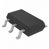
LTC1772BES6#TRM Linear Technology, LTC1772BES6#TRM Datasheet - Page 7

LTC1772BES6#TRM
Manufacturer Part Number
LTC1772BES6#TRM
Description
IC CTRLR DC/DC S-DWN SOT23-6
Manufacturer
Linear Technology
Type
Step-Down (Buck)r
Datasheet
1.LTC1772BES6TRMPBF.pdf
(16 pages)
Specifications of LTC1772BES6#TRM
Internal Switch(s)
No
Synchronous Rectifier
No
Number Of Outputs
1
Voltage - Output
0.8 ~ 9.8 V
Current - Output
1A
Frequency - Switching
550kHz
Voltage - Input
2.5 ~ 9.8 V
Operating Temperature
-40°C ~ 85°C
Mounting Type
Surface Mount
Package / Case
TSOT-23-6, TSOT-6
Lead Free Status / RoHS Status
Contains lead / RoHS non-compliant
Power - Output
-
Other names
LTC1772BES6#TRMTR
Available stocks
Company
Part Number
Manufacturer
Quantity
Price
OPERATION
that the external P-channel MOSFET will remain on for
more than one oscillator cycle since the inductor current
has not ramped up to the threshold set by EAMP . Further
reduction in input supply voltage will eventually cause the
P-channel MOSFET to be turned on 100%, i.e., DC. The
output voltage will then be determined by the input volt-
age minus the voltage drop across the MOSFET, the sense
resistor and the inductor.
Undervoltage Lockout
To prevent operation of the P-channel MOSFET below safe
input voltage levels, an undervoltage lockout is incorpo-
rated into the LTC1772B. When the input supply voltage
drops below approximately 2.0V, the P-channel MOSFET
and all circuitry is turned off except the undervoltage block,
which draws only several microamperes.
Short-Circuit Protection
When the output is shorted to ground, the frequency of
the oscillator will be reduced to about 120kHz. This lower
frequency allows the inductor current to safely discharge,
thereby preventing current runaway. The oscillator’s fre-
(Refer to Functional Diagram)
Figure 3. Maximum Output Current vs Duty Cycle
110
100
90
80
70
60
50
40
30
20
10
0
V
10 20 30 40 50
IN
= 4.2V
I
AT 5% DUTY CYCLE
I
AT 5% DUTY CYCLE
RIPPLE
RIPPLE
= 0.4I
= 0.2I
DUTY CYCLE (%)
PK
PK
quency will gradually increase to its designed rate when
the feedback voltage again approaches 0.8V.
Overvoltage Protection
As a further protection, the overvoltage comparator in
the LTC1772B will turn the external MOSFET off when
the feedback voltage has risen 7.5% above the reference
voltage of 0.8V. This comparator has a typical hysteresis
of 20mV.
Slope Compensation and Inductor’s Peak Current
The inductor’s peak current is determined by:
when the LTC1772B is operating below 40% duty
cycle. However, once the duty cycle exceeds 40%, slope
compensation begins and effectively reduces the peak
inductor current. The amount of reduction is given by the
curves in Figure 3.
60
I
PK
70 80 90 100
=
10
V
ITH
(
1772 F03
R
– . 0 85
SENSE
)
LTC1772B
1772bfa
7


