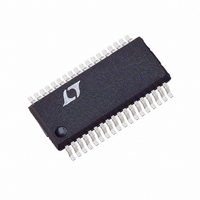
LTC3731HG Linear Technology, LTC3731HG Datasheet - Page 15

LTC3731HG
Manufacturer Part Number
LTC3731HG
Description
IC REG SW SYNC 3PH STPDWN 36SSOP
Manufacturer
Linear Technology
Series
PolyPhase®r
Type
Step-Down (Buck)r
Specifications of LTC3731HG
Internal Switch(s)
No
Synchronous Rectifier
Yes
Number Of Outputs
1
Voltage - Output
0.6 ~ 6 V
Frequency - Switching
225kHz ~ 680kHz
Voltage - Input
4 ~ 36 V
Operating Temperature
-40°C ~ 140°C
Mounting Type
Surface Mount
Package / Case
36-SSOP
Lead Free Status / RoHS Status
Contains lead / RoHS non-compliant
Current - Output
-
Power - Output
-
Lead Free Status / Rohs Status
Not Compliant
Available stocks
Company
Part Number
Manufacturer
Quantity
Price
Part Number:
LTC3731HG
Manufacturer:
LINEAR/凌特
Quantity:
20 000
Part Number:
LTC3731HG#PBF
Manufacturer:
LINEAR/凌特
Quantity:
20 000
Part Number:
LTC3731HG#TRPBF
Manufacturer:
LINEAR/凌特
Quantity:
20 000
applicaTions inForMaTion
Both MOSFETs have I
equation includes an additional term for transition losses,
which peak at the highest input voltage. For V
the high current efficiency generally improves with larger
MOSFETs, while for V
increase to the point that the use of a higher R
with lower C
synchronous MOSFET losses are greatest at high input
voltage when the top switch duty factor is low or during
a short circuit when the synchronous switch is on close
to 100% of the period.
The term (1 + d ) is generally given for a MOSFET in the
form of a normalized R
d = 0.005/°C can be used as an approximation for low
voltage MOSFETs.
The Schottky diodes (D1 to D3 in Figure 1) conduct during
the dead time between the conduction of the two large
power MOSFETs. This prevents the body diode of the bot-
tom MOSFET from turning on, storing charge during the
dead time and requiring a reverse recovery period which
could cost as much as several percent in efficiency. A 2A
to 8A Schottky is generally a good compromise for both
regions of operation due to the relatively small average
current. Larger diodes result in additional transition loss
due to their larger junction capacitance.
C
In continuous mode, the source current of each top
N-channel MOSFET is a square wave of duty cycle V
V
RMS current must be used. The details of a close form
equation can be found in Application Note 77. Figure 6
shows the input capacitor ripple current for different phase
configurations with the output voltage fixed and input volt-
age varied. The input ripple current is normalized against
the DC output current. The graph can be used in place of
tedious calculations. The minimum input ripple current
can be achieved when the product of phase number and
output voltage, N(V
input voltage V
IN
IN
. A low ESR input capacitor sized for the maximum
V
and C
V
OUT
IN
=
OUT
N
MILLER
k
Selection
where k
IN
or:
actually provides higher efficiency. The
OUT
2
IN
R losses while the topside N-channel
> 12V, the transition losses rapidly
DS(ON)
), is approximately equal to the
= 1 2
, , ..., –
vs temperature curve, but
N
1
DS(ON)
IN
< 12V,
device
OUT
/
So the phase number can be chosen to minimize the input
capacitor size for the given input and output voltages.
In the graph of Figure 4, the local maximum input RMS
capacitor currents are reached when:
These worst-case conditions are commonly used for design
because even significant deviations do not offer much relief.
Note that capacitor manufacturer’s ripple current ratings
are often based on only 2000 hours of life. This makes
it advisable to further derate the capacitor or to choose
a capacitor rated at a higher temperature than required.
Several capacitors may also be paralleled to meet size or
height requirements in the design. Always consult the
capacitor manufacturer if there is any question.
The Figure 6 graph shows that the peak RMS input current
is reduced linearly, inversely proportional to the number N
of stages used. It is important to note that the efficiency
loss is proportional to the input RMS current squared and
therefore a 3-stage implementation results in 90% less
power loss when compared to a single phase design. Bat-
tery/input protection fuse resistance (if used), PC board
trace and connector resistance losses are also reduced
by the reduction of the input ripple current in a PolyPhase
system. The required amount of input capacitance is further
V
V
OUT
IN
Figure 6. Normalized Input RMS Ripple Current
vs Duty Factor for One to Six Output Stages
=
0.6
0.5
0.4
0.3
0.2
0.1
2
0
k
0.1
N
–
1
0.2
where k
0.3
DUTY FACTOR (V
0.4
1-PHASE
2-PHASE
3-PHASE
4-PHASE
6-PHASE
12-PHASE
0.5
=
1 2
, , ...,
OUT
0.6
/V
IN
0.7
)
LTC3731H
N
0.8
3731H F06
0.9
3731Hfb


