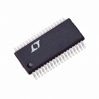
LTC3731HG Linear Technology, LTC3731HG Datasheet - Page 23

LTC3731HG
Manufacturer Part Number
LTC3731HG
Description
IC REG SW SYNC 3PH STPDWN 36SSOP
Manufacturer
Linear Technology
Series
PolyPhase®r
Type
Step-Down (Buck)r
Specifications of LTC3731HG
Internal Switch(s)
No
Synchronous Rectifier
Yes
Number Of Outputs
1
Voltage - Output
0.6 ~ 6 V
Frequency - Switching
225kHz ~ 680kHz
Voltage - Input
4 ~ 36 V
Operating Temperature
-40°C ~ 140°C
Mounting Type
Surface Mount
Package / Case
36-SSOP
Lead Free Status / RoHS Status
Contains lead / RoHS non-compliant
Current - Output
-
Power - Output
-
Lead Free Status / Rohs Status
Not Compliant
Available stocks
Company
Part Number
Manufacturer
Quantity
Price
Part Number:
LTC3731HG
Manufacturer:
LINEAR/凌特
Quantity:
20 000
Part Number:
LTC3731HG#PBF
Manufacturer:
LINEAR/凌特
Quantity:
20 000
Part Number:
LTC3731HG#TRPBF
Manufacturer:
LINEAR/凌特
Quantity:
20 000
applicaTions inForMaTion
The power dissipation on the topside MOSFET can be
estimated. Using a Fairchild FDS6688 for example, R
= 7mΩ, C
voltage with T(estimated) = 50°C:
The worst-case power dissipation by the synchronous
MOSFET under normal operating conditions at elevated
ambient temperature and estimated 50°C junction tem-
perature rise is:
A short circuit to ground will result in a folded back
current of:
with a typical value of R
= 0.25. The resulting power dissipated in the bottom
MOSFET is:
which is less than one third of the normal, full load con-
ditions. Incidentally, since the load no longer dissipates
any power, total system power is decreased by over 90%.
Therefore, the system actually cools significantly during
a shorted condition!
PC Board Layout Checklist
When laying out the printed circuit board, the following
checklist should be used to ensure proper operation of
the IC. These items are also illustrated graphically in the
layout diagram of Figure 11. Check the following in the
PC layout:
P
P
P
I
SC
MAIN
SYNC
SYNC
≈
(
= (7.5A)
MILLER
≈
=
2 3
0 007
25
1 8
+
20
20
.
5
.
mV
V
V
V
)
V
20
m
= 15nC/15V = 1000pF . At maximum input
– .
−
( )
Ω
1
2
15 1
Ω
1 8
V
1 3
(1.25)(0.007Ω) ≈ 0.5W
+
.
+
2
V
( )
V
20
[
2
1
+
(
DS(ON)
15
+
1 8
2
150
(
.
A
0 005 50
1
( )( )
) (
.
0 6
V
45
2 3
2
ns
.
and d = (0.005/°C)(50°C)
1 25 0 007
(
µ
A
(
.
400
20
)
H
(
Ω
V
( )(
)
2
kHz
(
)
° −
=
C
.
)
1000
7 5
=
25
.
Ω
2 2
°
A
.
)
C
pF
=
)
W
]
1 84
DS(ON)
)
.
W
1) Are the signal and power ground paths isolated? Keep
the SGND at one end of a printed circuit path thus prevent-
ing MOSFET currents from traveling under the IC. The IC
signal ground pin should be used to hook up all control
circuitry on one side of the IC, routing the copper through
SGND, under the IC covering the “shadow” of the package,
connecting to the PGND pin and then continuing on to the
(–) plates of C
should be placed immediately adjacent to the IC between
the V
or X5R type is small enough to fit very close to the IC to
minimize the ill effects of the large current pulses drawn
to drive the bottom MOSFETs. An additional 5µF to 10µF
of ceramic, tantalum or other very low ESR capacitance is
recommended in order to keep the internal IC supply quiet.
The power ground returns to the sources of the bottom
N-channel MOSFETs, anodes of the Schottky diodes and
(–) plates of C
as possible.
2) Does the V
sistors? The resistive divider R1/R2 must be connected
between the (+) plate of C
3) Are the SENSE
each channel routed together with minimum PC trace spac-
ing? The filter capacitors between SENSE
each channel should be as close as possible to the pins of
the IC. Connect the SENSE
of the sense resistor as illustrated in Figure 12.
4) Do the (+) plates of C
topside MOSFETs as closely as possible? This capacitor
provides the pulsed current to the MOSFETs.
5) Keep the switching nodes, SWITCH, BOOST and TG
away from sensitive small-signal nodes (SENSE
EAIN). Ideally the SWITCH, BOOST and TG printed circuit
traces should be routed away and separated from the IC
and especially the “quiet” side of the IC. Separate the high
dv/dt traces from sensitive small-signal nodes with ground
traces or ground planes.
6) Use a low impedance source such as a logic gate to drive
the PLLIN pin and keep the lead as short as possible.
CC
pin and PGND. A 1µF ceramic capacitor of the X7R
IN
FB
IN
, which should have as short lead lengths
and C
pin connect directly to the feedback re-
–
and SENSE
OUT
PWR
. The V
OUT
–
and SENSE
connect to the drains of the
and signal ground.
+
printed circuit traces for
CC
decoupling capacitor
LTC3731H
+
+
pins to the pads
and SENSE
+
, SENSE
3731Hfb
–
for
–
,


