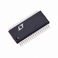
LTC3731HG Linear Technology, LTC3731HG Datasheet - Page 26

LTC3731HG
Manufacturer Part Number
LTC3731HG
Description
IC REG SW SYNC 3PH STPDWN 36SSOP
Manufacturer
Linear Technology
Series
PolyPhase®r
Type
Step-Down (Buck)r
Specifications of LTC3731HG
Internal Switch(s)
No
Synchronous Rectifier
Yes
Number Of Outputs
1
Voltage - Output
0.6 ~ 6 V
Frequency - Switching
225kHz ~ 680kHz
Voltage - Input
4 ~ 36 V
Operating Temperature
-40°C ~ 140°C
Mounting Type
Surface Mount
Package / Case
36-SSOP
Lead Free Status / RoHS Status
Contains lead / RoHS non-compliant
Current - Output
-
Power - Output
-
Lead Free Status / Rohs Status
Not Compliant
Available stocks
Company
Part Number
Manufacturer
Quantity
Price
Part Number:
LTC3731HG
Manufacturer:
LINEAR/凌特
Quantity:
20 000
Part Number:
LTC3731HG#PBF
Manufacturer:
LINEAR/凌特
Quantity:
20 000
Part Number:
LTC3731HG#TRPBF
Manufacturer:
LINEAR/凌特
Quantity:
20 000
LTC3731H
applicaTions inForMaTion
The worst-case input RMS ripple current for a single stage
design peaks at twice the value of the output voltage. The
worst-case input RMS ripple current for a two stage design
results in peaks at 1/4 and 3/4 of the input voltage, and
the worst-case input RMS ripple current for a three stage
design results in peaks at 1/6, 1/2, and 5/6 of the input
voltage. The peaks, however, are at ever decreasing levels
with the addition of more phases. A higher effective duty
factor results because the duty factors “add” as long as
the currents in each stage are balanced. Refer to AN19
for a detailed description of how to calculate RMS current
for the single stage switching regulator.
Figure 6 illustrates the RMS input current drawn from the
input capacitance versus the duty cycle as determined by
the ratio of input and output voltage. The peak input RMS
current level of the single phase system is reduced by 2/3
in a 3-phase solution due to the current splitting between
the three stages.
The output ripple current is reduced significantly when
compared to the single phase solution using the same
inductance value because the V
term from the stages that has their bottom MOSFETs on
subtract current from the (V
resulting from the stage which has its top MOSFET on.
The output ripple current for a 3-phase design is:
The ripple frequency is also increased by three, further re-
ducing the required output capacitance when V
as illustrated in Figure 6.
The addition of more phases, by phase locking addi-
tional controllers, always results in no net input or output
ripple at V
implemented. Designing a system with multiple stages
close to the V
ripple voltage at the input and outputs and thereby improve
efficiency, physical size and heat generation of the overall
switching power supply. Refer to Application Note 77 for
more information on Polyphase circuits.
I
P-P
=
( )( )
V
OUT
f L
OUT
/V
OUT
(
IN
1 3
/V
–
ratios equal to the number of stages
IN
DC
ratio will significantly reduce the
)
CC
V
IN
– V
>
OUT
OUT
3
V
/L discharge currents
OUT
)/L charging current
CC
< 3V
OUT
Efficiency Calculation
To estimate efficiency, the DC loss terms include the input
and output capacitor ESR, each MOSFET R
resistance R
drop of the Schottky rectifier at the operating output current
and temperature. Typical values for the design example
given previously in this data sheet are:
The main MOSFET is on for the duty factor V
the synchronous MOSFET is on for the rest of the period
or simply (1 – V
small, the AC loss in the inductor can be made small if
a good quality inductor is chosen. The average current,
I
below is not exact but should provide a good technique
for the comparison of selected components and give a
result that is within 10% to 20% of the final application.
Determining the MOSFETs’ die temperature may require
iterative calculations if one is not familiar with typical
performance. A maximum operating junction temperature
of 90° to 100°C for the MOSFETs is recommended for
high reliability applications.
Common output path DC loss:
This totals 3.7W + C
P
OUT
COMPATH
Main MOSFET R
Sync MOSFET R
C
C
R
R
V
V
V
I
d = 0.5%°C (MOSFET temperature coefficient)
N = 3
f = 400kHz
MAX
, is used to simplify the calculations. The equation
INESR
OUTESR
SCHOTTKY
OUT
IN
L
SENSE
= 2.5mΩ
= 12V
= 45A
= 1.3V
= 20mΩ
= 3mΩ
≈
= 3mΩ
L
N
, the sense resistance R
= 0.8V at 15A (0.7V at 90°C)
I
OUT
MAX
N
DS(ON)
DS(ON)
/V
OUTESR
IN
2
). Assuming the ripple current is
(
R
= 7mΩ (9mΩ at 90°C)
= 7mΩ (9mΩ at 90°C)
L
loss.
+
R
SENSE
SENSE
)
+
C
DS(ON)
and the forward
OUTESR
OUT
, inductor
/V
Lo
IN
3731Hfb
s s s
and


