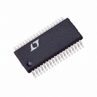
LTC3731HG Linear Technology, LTC3731HG Datasheet - Page 25

LTC3731HG
Manufacturer Part Number
LTC3731HG
Description
IC REG SW SYNC 3PH STPDWN 36SSOP
Manufacturer
Linear Technology
Series
PolyPhase®r
Type
Step-Down (Buck)r
Specifications of LTC3731HG
Internal Switch(s)
No
Synchronous Rectifier
Yes
Number Of Outputs
1
Voltage - Output
0.6 ~ 6 V
Frequency - Switching
225kHz ~ 680kHz
Voltage - Input
4 ~ 36 V
Operating Temperature
-40°C ~ 140°C
Mounting Type
Surface Mount
Package / Case
36-SSOP
Lead Free Status / RoHS Status
Contains lead / RoHS non-compliant
Current - Output
-
Power - Output
-
Lead Free Status / Rohs Status
Not Compliant
Available stocks
Company
Part Number
Manufacturer
Quantity
Price
Part Number:
LTC3731HG
Manufacturer:
LINEAR/凌特
Quantity:
20 000
Part Number:
LTC3731HG#PBF
Manufacturer:
LINEAR/凌特
Quantity:
20 000
Part Number:
LTC3731HG#TRPBF
Manufacturer:
LINEAR/凌特
Quantity:
20 000
applicaTions inForMaTion
of the input capacitor and not share a common ground
path with any switched current paths. The left half of the
circuit gives rise to the “noise” generated by a switching
regulator. The ground terminations of the synchronous
MOSFETs and Schottky diodes should return to the bot-
tom plate(s) of the input capacitor(s) with a short isolated
PC trace since very high switched currents are present.
A separate isolated path from the bottom plate(s) of the
input and output capacitor(s) should be used to tie in the IC
power ground pin (PGND). This technique keeps inherent
signals generated by high current pulses taking alternate
current paths that have finite impedances during the total
period of the switching regulator. External OPTI-LOOP
compensation allows overcompensation for PC layouts
which are not optimized but this is not the recommended
design procedure.
Figure 13. Single and Polyphase Current Waveforms
I
I
V
V
V
COUT
COUT
V
SW1
SW2
SW3
I
I
CIN
CIN
SW
I
I
I
L1
L2
L3
SINGLE PHASE
TRIPLE PHASE
Simplified Visual Explanation of How a 3-Phase
Controller Reduces Both Input and Output RMS
Ripple Current
The effect of multiphase power supply design significantly
reduces the amount of ripple current in both the input and
output capacitors. The RMS input ripple current is divided
by, and the effective ripple frequency is multiplied up by
the number of phases used (assuming that the input volt-
age is greater than the number of phases used times the
output voltage). The output ripple amplitude is also reduced
by, and the effective ripple frequency is increased by the
number of phases used. Figure 13 graphically illustrates
the principle.
3731H F13
LTC3731H
3731Hfb


