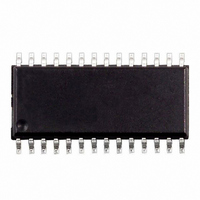
L6712D STMicroelectronics, L6712D Datasheet - Page 13

L6712D
Manufacturer Part Number
L6712D
Description
IC CTRLR DC/DC 2PHASE 28-SOIC
Manufacturer
STMicroelectronics
Type
Step-Down (Buck)r
Datasheet
1.L6712AQTR.pdf
(29 pages)
Specifications of L6712D
Internal Switch(s)
No
Synchronous Rectifier
Yes
Number Of Outputs
2
Voltage - Output
0.9 ~ 3.3 V
Current - Output
2A
Frequency - Switching
150kHz
Voltage - Input
12V
Operating Temperature
0°C ~ 70°C
Mounting Type
Surface Mount
Package / Case
28-SOIC (7.5mm Width)
Power - Output
2W
Operating Temperature Range
- 40 C to + 125 C
Mounting Style
SMD/SMT
Lead Free Status / RoHS Status
Lead free / RoHS Compliant
Other names
497-5364-5
L6712D
L6712D
Available stocks
Company
Part Number
Manufacturer
Quantity
Price
Company:
Part Number:
L6712D
Manufacturer:
ATMEL
Quantity:
6 822
Part Number:
L6712D
Manufacturer:
ST
Quantity:
20 000
Company:
Part Number:
L6712DTR
Manufacturer:
ST
Quantity:
3 683
Since the device senses the output current across the low-side mosfets (or across a sense resistors in
series with them) the device limits the bottom of the inductor current triangular waveform: an over current
is detected when the current flowing into the sense element is greater than I
■
The maximum duty cycle is limited as a function of the measured current and, since the oscillator frequen-
cy is fixed once programmed, imply a maximum on-time limitation as follow (where T is the switching pe-
riod T=1/f
This linear dependence has a value at zero load of 0.80·T and at maximum current of 0.40·T typical and
results in two different behaviors of the device:
Figure 9. TON Limited Operation
T
This happens when the maximum ON time is reached before the current in each phase reaches I
FOx
Figure 9a shows the maximum output voltage that the device is able to regulate considering the T
itation imposed by the previous relationship. If the desired output characteristic crosses the T
maximum output voltage, the output resulting voltage will start to drop after crossing. In this case, the de-
vice doesn't perform constant current limitation but only limits the maximum duty cycle following the pre-
vious relationship. The output voltage follows the resulting characteristic (dotted in Figure 9b) until UVP is
detected or anyway until I
Constant Current Operation
This happens when ON time limitation is reached after the current in each phase reaches I
35µA).
The device enters in Quasi-Constant-Current operation: the low-side mosfets stays ON until the current
read becomes lower than I
ON with a TON imposed by the control loop at the next available clock cycle and the device works in the
T
ON
ON,MAX
L6712 - Dynamic Maximum Duty Cycle Limitation
0.80·V
0.40·V
< 35µA).
Limited Output Voltage.
V
OUT
IN
IN
SW
=
a ) Maximum output Voltage
(
and I
0.80 I
OUT
–
FB
T
is the output current):
ON
I
⋅
OCPx
5.73k
Limited Output
FB
OCPx
characteristic
(I
= 70µA.
I
DROOP
OCP
=
) T
(I
=2·I
⋅
INFOx
35µA Rg
-------------------------- -
=70µA)
R
OCPx
=
SENSE
⎛
⎝
< 35µA) skipping clock cycles. The high side mosfets can be turned
0.80
⋅
I
OUT
–
R
--------------------- - I
SENSE
Rg
⋅
Rg
OUT
0.80·V
0.40·V
=
V
OUT
⋅
I
------------------------------------------ -
OCPx
IN
IN
5.73k
b) TON Limited Output Voltage
35µA
⋅
⎞ T =
⎠
R
⋅
SENSE
⎧
⎪
⎨
⎪
⎩
OCPx
T
T
=
=
(I
0.80 T I
0.40 T I
(I
INFOx
I
DROOP
OCP
=2·I
characteristic and
L6712A L6712
⋅
⋅
Resulting Output
=70 µ A)
> 35µA).
Desired Output
OCPx
UVP threshold
characteristic
OCPx
FB
FB
I
ON
OUT
=
=
OCPx
(I
0µA
70µA
INFOx
ON
limited
13/29
(I
lim-
IN-
>


