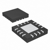
MAX15037ATE+T Maxim Integrated Products, MAX15037ATE+T Datasheet - Page 11

MAX15037ATE+T
Manufacturer Part Number
MAX15037ATE+T
Description
IC DC/DC CONV 3A 16-TQFN-EP
Manufacturer
Maxim Integrated Products
Type
Step-Down (Buck)r
Datasheet
1.MAX15036ATEVT.pdf
(25 pages)
Specifications of MAX15037ATE+T
Internal Switch(s)
Yes
Synchronous Rectifier
Yes
Number Of Outputs
1
Voltage - Output
0.6 ~ 23 V
Current - Output
3A
Frequency - Switching
200kHz ~ 2.2MHz
Voltage - Input
4.5 ~ 23 V
Operating Temperature
-40°C ~ 125°C
Mounting Type
Surface Mount
Package / Case
16-TQFN Exposed Pad
Power - Output
2.67W
Lead Free Status / RoHS Status
Lead free / RoHS Compliant
The MAX15036/MAX15037 use a pulse-width modula-
tion (PWM) voltage-mode control scheme. The
MAX15036 is a nonsynchronous converter and uses an
external low-forward-drop Schottky diode for rectifica-
tion. The MAX15037 is a synchronous converter and
drives a low-side, low-gate-charge MOSFET for higher
efficiency. The controller generates the clock signal
from an internal oscillator or the SYNC input when dri-
ven by an external clock. An internal transconductance
error amplifier produces an integrated error voltage at
COMP, providing high DC accuracy. The voltage at
COMP sets the duty cycle using a PWM comparator
and an internal 1V
edge of the clock, the converter’s high-side n-channel
MOSFET turns on and remains on until either the
appropriate or maximum duty cycle is reached or the
maximum current limit for the switch is detected.
In the case of the MAX15036 boost operation, the
MOSFET is a low-side switch. During each on-time, the
inductor current ramps up. During the second half of
the switching cycle, the low-side switch turns off and
forward biases the Schottky diode. During this time, the
DRAIN voltage is clamped to 0.4V (V
and the inductor provides energy to the output as well
as replenishes the output capacitor charge.
During each high-side MOSFET on-time (Figure 5), the
inductor current ramps up. During the second half of the
switching cycle, the high-side MOSFET turns off and for-
ward biases the Schottky rectifier (D2 in Figure 5). During
this time, the SOURCE voltage is clamped to 0.5V below
ground. The inductor releases the stored energy as its
current ramps down, and provides current to the output.
During the MOSFET off-time, when the Schottky rectifier is
conducting, the bootstrap capacitor (C10 in Figure 5) is
recharged from the V
MAX15036 goes in to discontinuous conduction mode
operation when the inductor current completely dis-
charges before the next switching cycle commences.
When the MAX15036 operates in discontinuous conduc-
tion, the bootstrap capacitor can become undercharged.
To prevent this, an internal low-side 20Ω switch (see N3 in
Figure 1) turns on, during the off-time, once every 4 clock
cycles. This ensures that the negative terminal of the boot-
strap capacitor is pulled to PGND often enough to allow it
to fully charge to V
properly turns on. The operation of the bootstrap capaci-
tor wake-up switch causes a small increase in the output
voltage ripple at light loads. Under overload conditions,
______________________________________________________________________________________
L
P-P
, ensuring the internal power switch
Detailed Description
voltage ramp. At each rising
L
2.2MHz, 3A Buck or Boost Converters
output. At light loads, the
with an Integrated High-Side Switch
PWM Controller
D
) above V
MAX15036
OUT
when the inductor current exceeds the peak current limit
of the internal switch, the high-side MOSFET turns off
quickly and waits until the next clock cycle.
The MAX15037 is intended for synchronous buck oper-
ation only. During the high-side MOSFET on-time, the
inductor current ramps up. When the MOSFET turns off,
the inductor reverses polarity and forward biases the
Schottky rectifier in parallel with the low-side synchro-
nous MOSFET. The SOURCE voltage is clamped to
0.5V below ground until the break-before-make time
(t
tifier MOSFET turns on. The inductor releases the
stored energy as its current ramps down, and contin-
ues providing current to the output. The bootstrap
capacitor is also recharged from the V
the MOSFET turns off. The synchronous rectifier keeps
the circuit in continuous conduction mode operation
even at light load. Under overload conditions, when the
inductor current exceeds the peak current limit of the
internal switch, the high-side MOSFET turns off and
waits until the next clock cycle.
The MAX15037, with the synchronous rectifier driver out-
put (DL), has an adaptive break-before-make circuit to
avoid cross conduction between the internal power
MOSFET and the external synchronous rectifier MOSFET.
When the synchronous rectifier MOSFET is turning off, the
internal high-side power MOSFET is kept off until V
below 0.97V. Similarly, DL does not go high until the inter-
nal power MOSFET gate voltage falls below 1.24V.
All internal control circuitry operates from an internally reg-
ulated nominal voltage of 5.2V (V
ages (V+) of 5.5V to 23V, V
or below, the internal linear regulator operates in dropout
mode, where V
the dropout voltage can be high enough to reduce V
below the undervoltage lockout (UVLO) threshold.
For input voltages of lower than 5.5V, connect V+ and
V
switching frequency of the converter. See the V
Output Voltage vs. Switching Frequency graph in the
Typical Operating Characteristics . For an input voltage
higher than 5.5V, use the internal regulator.
Bypass V+ to SGND with a low-ESR 0.1μF or greater
ceramic capacitor placed as close as possible to the
MAX15036/MAX15037. Current spikes from V
the internal circuitry powered by V
low-ESR 0.1μF ceramic capacitor to PGND and a low-
ESR 4.7μF ceramic capacitor to SGND.
BBM
L
together. The load on V
) of 25ns is over. After t
Input Voltage (V+)/Internal Linear
L
follows V+. Depending on the load on V
L
is regulated to 5.2V. At 5.5V
BBM,
L
is proportional to the
L
). At higher input volt-
the synchronous rec-
L
. Bypass V
Regulator (V
L
MAX15037
output when
L
L
disturb
DL
with a
falls
L
L
11
to
L
L
)
,


