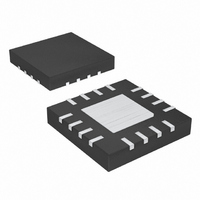
MAX15037ATE+T Maxim Integrated Products, MAX15037ATE+T Datasheet - Page 17

MAX15037ATE+T
Manufacturer Part Number
MAX15037ATE+T
Description
IC DC/DC CONV 3A 16-TQFN-EP
Manufacturer
Maxim Integrated Products
Type
Step-Down (Buck)r
Datasheet
1.MAX15036ATEVT.pdf
(25 pages)
Specifications of MAX15037ATE+T
Internal Switch(s)
Yes
Synchronous Rectifier
Yes
Number Of Outputs
1
Voltage - Output
0.6 ~ 23 V
Current - Output
3A
Frequency - Switching
200kHz ~ 2.2MHz
Voltage - Input
4.5 ~ 23 V
Operating Temperature
-40°C ~ 125°C
Mounting Type
Surface Mount
Package / Case
16-TQFN Exposed Pad
Power - Output
2.67W
Lead Free Status / RoHS Status
Lead free / RoHS Compliant
For the boost converter:
The power lost due to switching the internal power
MOSFET is:
t
MOSFET measured at SOURCE.
The power lost due to the switching quiescent current
of the device is:
The switching quiescent current (I
MAX15036/MAX15037 is dependent on switching fre-
quency. See the Typical Operating Characteristics sec-
tion for the value of I
In the case of the MAX15037, the switching current
includes the synchronous rectifier MOSFET gate-drive
current (I
charge (Q
and the switching frequency.
where the Q
nous rectifier MOSFET at V
The total power dissipated in the device is:
Calculate the temperature rise of the die using the fol-
lowing equation:
R
I
and t
RMS_MOSFET
F
P
Q
SW-DL
are the rise and fall times of the internal power
g-DL
= V
P
P
g-DL
I
SW
P
SW-DL
TOTAL
Q
IN
) of the synchronous rectifier MOSFET
). The I
=
=
= V
x (I
is the total gate charge of the synchro-
ΔI
______________________________________________________________________________________
V
(
IN
= Q
I
P P
IN
= P
SW
2
SW
−
DC
I
I
×
DC
PK
x I
SW-DL
I
IN
I
g-DL
MOSFET
OUT
at a given frequency.
+ I
=
+I
2.2MHz, 3A Buck or Boost Converters
SW
=
=
=
2
(
SW-DL
GS
I
I
V
IN
IN
PK
with an Integrated High-Side Switch
V
IN
×
x f
OUT
depends on the total gate
(
+
4
= 5V.
−
V
+(I
t
SW
−
R
L
IN
+ P
Δ
Δ
V
)
+
×
I
I
DC
DROP
P P
P P
×
2
2
× η
t
−
−
SW
f
I
F
OUT
SW
×
)
×
I
PK
+ P
)
f
SW
×
))
Q
D
SW
×
(MAX15036)
(MAX15037)
D
) of the
MAX
3
θ
1.7°C/W. T
the junction temperature, or die temperature. The case-
to-ambient thermal resistance is dependent on how
well heat can be transferred from the PCB to the air.
Solder the underside exposed pad to a large copper
GND plane. If the die temperature reaches +170°C the
MAX15036/MAX15037 shut down and do not restart
again until the die temperature cools by 25°C.
The MAX15036/MAX15037 have an internal transcon-
ductance error amplifier with an inverting input (FB)
and output (COMP) available for external frequency
compensation. The flexibility of external compensation
and high switching frequencies for the MAX15036/
MAX15037 allow a wide selection of output filtering
components, especially the output capacitor. For cost-
sensitive applications, use high-ESR aluminum elec-
trolytic capacitors. For size-sensitive applications, use
low-ESR tantalum or ceramic capacitors at the output.
Before designing the compensation components, first
choose all the passive power components that meet
the output ripple, component size, and component cost
requirements. Secondly, choose the compensation
components to achieve the desired closed-loop band-
width and phase margin. Use a simple 1-zero, 2-pole
pair (Type II) compensation if the output capacitor ESR
zero frequency (f
crossover frequency (f
III) compensation when the f
Use procedure 1 to calculate the compensation net-
work components when f
Procedure 1 (see Figure 3)
Calculate the f
Calculate the unity-gain crossover frequency as:
JC
is the junction-to-case thermal resistance equal to
C
is the temperature of the case and T
ZESR
f
f
T
ZESR
LC
J
= T
=
and f
ZESR
2
=
C
π
Buck Converter Compensation
2
+ (P
C
×
f
C
π
). Use a 2-zero, 2-pole (Type
ZESR
LC
×
=
) is below the unity-gain
L C
TOTAL
ESR C
double pole:
1
ZESR
f
×
SW
20
< f
1
OUT
×
C
is higher than f
x θ
.
OUT
Compensation
JC
)
C
.
J
17
is


