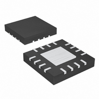
MAX15037ATE+T Maxim Integrated Products, MAX15037ATE+T Datasheet - Page 8

MAX15037ATE+T
Manufacturer Part Number
MAX15037ATE+T
Description
IC DC/DC CONV 3A 16-TQFN-EP
Manufacturer
Maxim Integrated Products
Type
Step-Down (Buck)r
Datasheet
1.MAX15036ATEVT.pdf
(25 pages)
Specifications of MAX15037ATE+T
Internal Switch(s)
Yes
Synchronous Rectifier
Yes
Number Of Outputs
1
Voltage - Output
0.6 ~ 23 V
Current - Output
3A
Frequency - Switching
200kHz ~ 2.2MHz
Voltage - Input
4.5 ~ 23 V
Operating Temperature
-40°C ~ 125°C
Mounting Type
Surface Mount
Package / Case
16-TQFN Exposed Pad
Power - Output
2.67W
Lead Free Status / RoHS Status
Lead free / RoHS Compliant
2.2MHz, 3A Buck or Boost Converters
with an Integrated High-Side Switch
8
PIN
1, 2
10
11
12
13
14
15
16
—
3
4
5
6
7
8
9
_______________________________________________________________________________________
BST/VDD
SOURCE
BYPASS
PGOOD
DRAIN
RESET
NAME
COMP
SGND
PGND
SYNC
CKO
OSC
EN
FB
V+
DL
EP
V
L
Internal Power MOSFET Drain Connection. Buck converter operation—use the MOSFET as a high-side switch
and connect DRAIN to the input supply. Boost converter operation (MAX15036 only)—use the MOSFET as a
low-side switch and connect DRAIN to the inductor and diode junction.
Transconductance Error Amplifier Output. Connect a compensation network from COMP to SGND or from
COMP to FB to SGND (see the Compensation section).
Feedback Input. Connect a resistive divider from the output to FB to SGND to set the output voltage.
Switching Frequency Set Input. Connect a resistor R
When using external synchronization, program R
required when external synchronization is used.
Reference Bypass Connection. Bypass to SGND with a 0.22μF or greater ceramic capacitor.
Input Supply Voltage. V+ can range from 5.5V to 23V. Connect V+ and V
operation. Bypass V+ to SGND with a minimum of 0.1μF ceramic capacitor.
Internal Regulator Output. Bypass V
ceramic capacitor. Connect V+ to V
Clock Output (MAX15036 Only). CKO is an output with the same frequency as the converter’s switching
frequency and 115° out-of-phase. CKO is used to synchronize the MAX15036 to other MAX15036/MAX15037s.
Low-Side Synchronous Rectifier Driver (MAX15037 Only). DL sources 0.7A and sinks 1A to quickly turn on and
off the external synchronous rectifier MOSFET.
Signal Ground
Power Ground. Connect the rectifier diode’s anode, the input capacitor negative terminal, the output capacitor
negative terminal, and V
Internal Power MOSFET Source Connection. Buck converter operation—connect SOURCE to the switched side
of the inductor as shown in Figure 5. Boost converter operation (MAX15036 only)—connect SOURCE to PGND.
External Synchronization Input. Connect SYNC to an external logic-level clock to synchronize the MAX15036/
MAX15037. Connect SYNC to SGND when not used.
Open-Drain Active-Low Reset Output (MAX15036 Only). RESET remains low while the converter’s output is
below 92.5% of V
high after the reset timeout period of 200ms (typ).
Open-Drain Power-Good Output (MAX15037 Only). PGOOD remains low while the output is below 92.5% of its
nominal set point.
Internal MOSFET Driver Supply Input. Buck converter operation—bootstrap flying capacitor connection.
Connect BST/VDD to an external ceramic capacitor and diode (see Figure 5). Boost converter operation
(MAX15036 only)—driver bypass capacitor connection. Connect a low-ESR 0.1μF ceramic capacitor from
BST/VDD to PGND.
Enable Input. A logic-low turns off the converter. A logic-high turns on the device. Connect EN to V
always-on application.
Exposed Pad. Connect to SGND. Solder EP to SGND to enhance thermal dissipation.
OUT
’s nominal set point. When V
L
bypass capacitor negative terminal to PGND.
L
L
for 4.5V to 5.5V operation.
to SGND with a 4.7μF ceramic capacitor and to PGND with a 0.1μF
OSC
OUT
FUNCTION
OSC
so that (0.8 x f
rises above 92.5% of its nominal set point, RESET goes
from OSC to SGND to set the switching frequency.
SYNC
) ≤ f
L
together for 4.5V to 5.5V input
SW
≤ (1.2 x f
Pin Description
SYNC
). R
OSC
L
for an
is still


