L6710 STMicroelectronics, L6710 Datasheet - Page 24

L6710
Manufacturer Part Number
L6710
Description
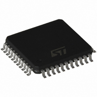
IC CTRLR 6BIT 2PH PROGR 44-TQFP
Manufacturer
STMicroelectronics
Type
Step-Down (Buck)r
Datasheet
1.L6710.pdf
(34 pages)
Specifications of L6710
Internal Switch(s)
No
Synchronous Rectifier
Yes
Number Of Outputs
2
Voltage - Output
0.84 ~ 1.6 V
Current - Output
2A
Frequency - Switching
150kHz
Voltage - Input
12V
Operating Temperature
0°C ~ 125°C
Mounting Type
Surface Mount
Package / Case
44-TQFP, 44-VQFP
Power - Output
2.5W
Product
Half-Bridge Drivers
Supply Current
12.5 mA
Mounting Style
SMD/SMT
Lead Free Status / RoHS Status
Lead free / RoHS Compliant
Available stocks
Company
Part Number
Manufacturer
Quantity
Price
Company:
Part Number:
L671000
Manufacturer:
PHI
Quantity:
1 870
Part Number:
L671000
Manufacturer:
OKI
Quantity:
20 000
L6710
Figure 17. Device orientation (left) and sense nets routing (right).
Gate resistors of few ohms help in reducing the power dissipated by the IC without compromising the sys-
tem efficiency.
The placement of other components is also important:
· The bootstrap capacitor must be placed as close as possible to the BOOTx and PHASEx pins to mini-
· Decoupling capacitor from VCC AND SGND placed as close as possible to the involved pins.
· Decoupling capacitor from VCCDR and PGND placed as close as possible to those pins. This capacitor
· Refer to SGND all the sensible components such as frequency set-up resistor (when present) and also
· Connect SGND to PGND on the load side (output capacitor) to avoid undesirable load regulation effect
· An additional 100nF ceramic capacitor is suggested to place near HS mosfet drain. This helps in reduc-
· Filtering VSEN pin vs. GND with 1nF capacitor helps in reducing noise injection into device.
· Filtering OUTEN pin vs. GND helps in reducing false trip due to coupled noise: take care in routing driv-
· PHASE pin spikes. Since the HS mosfet switches in hard mode, heavy voltage spikes can be observed
– Current Sense Connections.
· Remote Buffer: The input connections for this component must be routed as parallel nets from the
· Current Reading: The Rg resistors have to be placed as close as possible to the ISENx and PGNDS
24/34
mize the loop that is created.
sustains the peak currents requested by the low-side mosfet drivers.
the optional resistor from FB to GND used to give the positive droop effect.
and to ensure the right precision to the regulation when the remote sense buffer is not used. Connect
anyway in a single point (star grounding).
ing noise.
ing net for this pin in order to minimize coupled noise.
on the PHASE pins. If these voltage spikes overcome the max breakdown voltage of the pin, the device
can absorb energy and it can cause damages. The voltage spikes must be limited by proper layout, the
use of gate resistors, Schottky diodes in parallel to the low side mosfets and/or snubber network on the
low side mosfets, to a value lower than 26V, for 20nSec, at F
FBG/FBR pins to the load in order to compensate losses along the output power traces and also to
avoid the pick-up of any common mode noise. Connecting these pins in points far from the load will
cause a non-optimum load regulation, increasing output tolerance.
pins in order to limit the noise injection into the device. Moreover, PGNDS trace must be divided just
To HS Mosfet
(30 mils wide)
To LS Mosfets
(30 mils wide)
To HS Mosfet
(30 mils wide)
SW
of 600kHz max.


