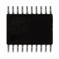
L6730C STMicroelectronics, L6730C Datasheet - Page 20

L6730C
Manufacturer Part Number
L6730C
Description
IC CTRLR ADJ STPDN SYNC 20-TSSOP
Manufacturer
STMicroelectronics
Type
Step-Down (Buck)r
Datasheet
1.L6730DTR.pdf
(50 pages)
Specifications of L6730C
Internal Switch(s)
No
Synchronous Rectifier
Yes
Number Of Outputs
1
Voltage - Output
Adj to 0.6V
Frequency - Switching
100kHz ~ 1MHz
Voltage - Input
1.8 ~ 14 V
Operating Temperature
-40°C ~ 85°C
Mounting Type
Surface Mount
Package / Case
20-TSSOP Exposed Pad, 20-eTSSOP, 20-HTSSOP
Package
HTSSOP20, QFN4x4 24L
For Use With
497-5868 - EVAL BOARD 30A 400KHZ L6730497-5501 - EVAL BOARD FOR L6730XX
Lead Free Status / RoHS Status
Lead free / RoHS Compliant
Current - Output
-
Power - Output
-
Device description
5.8
Figure 11. PGOOD signal
Figure 12. OVP not latched
20/50
Monitoring and protections
The output voltage is monitored by the FB pin. If it is not within ±10% (typ.) of the programmed
value, the Power-Good (PGOOD) output is forced low. The PGOOD signal can be delayed by
adding an external capacitor on PGDelay pin (see
this can be useful to perform cascade sequencing. The delay can be calculated with the
following formula:
The device provides over-voltage-protection: when the voltage sensed on FB pin reaches a
value 20% (typ.) greater than the reference, the low-side driver is turned on. If the OVP not-
latched mode has been set the low-side MOSFET is kept on as long as the over voltage is
detected (see
on until Vcc is toggled (see
high (4.5V typ.) if an over voltage is detected. .
Figure
12.).If OVP latched-mode has been set the low-side MOSFET is turned
PGDelay
Figure
13.). In case of latched-mode OVP the OSC pin is forced
0
5 .
C
pF
Table 3: Pins connection
[pF] (3)
L6730C - L6730D
OSC
and
LGate
FB
Figure
11.);


