DS1990A-F3+ Maxim Integrated Products, DS1990A-F3+ Datasheet - Page 7
DS1990A-F3+
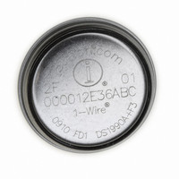
Manufacturer Part Number
DS1990A-F3+
Description
IC IBUTTON SERIAL NUMBER F3
Manufacturer
Maxim Integrated Products
Series
iButton®r
Type
Serial Number IButtonr
Datasheet
1.DS1990A-F5.pdf
(10 pages)
Specifications of DS1990A-F3+
Rohs Information
IButton RoHS Compliance Plan
Memory Size
8B
Memory Type
ROM
Maximum Operating Temperature
+ 85 C
Package / Case
F3 MicroCan
Minimum Operating Temperature
- 40 C
Mounting Style
SMD/SMT
Ic Function
Serial Number IButton IC
Supply Voltage Range
2.8V To 6V
Operating Temperature Range
-40°C To +85°C
Digital Ic Case Style
F3 IButton
Termination Type
SMD
Supply Voltage Min
2.8V
Rohs Compliant
Yes
Filter Terminals
SMD
Lead Free Status / RoHS Status
Lead free / RoHS Compliant


The DS1990A requires strict protocols to ensure data
integrity. The protocol consists of four types of signaling
on one line: reset sequence with reset pulse and pres-
ence pulse, write-zero, write-one, and read-data.
Except for the presence pulse, the bus master initiates
all these signals.
To get from idle to active, the voltage on the 1-Wire line
needs to fall from V
active to idle, the voltage needs to rise from V
above V
this rise, referenced as ε in Figure 6, depends on the
value of the pullup resistor (R
the 1-Wire network attached.
The initialization sequence required to begin any com-
munication with the DS1990A is shown in Figure 6. A
reset pulse followed by a presence pulse indicates that
the DS1990A is ready to receive a ROM function com-
mand. If the bus master uses slew-rate control on the
falling edge, it must pull down the line for t
compensate for the edge.
After the bus master has released the line, it goes into
receive mode (Rx). Now the 1-Wire bus is pulled to
V
DS2480B driver, by active circuitry. When the V
crossed, the DS1990A waits for t
a presence pulse by pulling the line low for t
Figure 6. Initialization Procedure: Reset and Presence Pulses
PUP
through the pullup resistor or, in the case of a
IHMIN
V
V
ILMAX
IHMIN
V
PUP
. The time it takes for the voltage to make
0V
_______________________________________________________________________________________
PUP
t
F
to below V
MASTER Tx "RESET PULSE"
RESISTOR
1-Wire Signaling
PUP
PDH
) and capacitance of
ILMAX
and then transmits
t
RSTL
. To get from
RSTL
ILMAX
IHMIN
PDL
+ t
. To
F
to
to
is
ε
MASTER
detect a presence pulse, the master must test the logi-
cal state of the 1-Wire line at t
Data communication with the DS1990A takes place in
time slots that carry a single bit each. Write time slots
transport data from bus master to slave. Read time
slots transfer data from slave to master. The definitions
of the write and read time slots are illustrated in
Figure 7.
All communication begins with the master pulling the
data line low. As the voltage on the 1-Wire line falls
below V
generator that determines when the data line is sam-
pled during a write time slot and how long data is valid
during a read time slot.
For a write-one time slot, the voltage on the data line
must have risen above V
time t
voltage on the data line must stay below V
the write-zero low time t
able communication, the voltage on the data line
should not exceed V
dow. After the voltage has risen above V
DS1990A needs a recovery time t
for the next time slot.
Serial Number iButton
t
PDH
W1LMAX
t
MSP
ILMAX
MASTER Rx "PRESENCE PULSE"
t
PDL
t
RSTH
is expired. For a write-zero time slot, the
, the DS1990A starts its internal timing
ILMAX
W0LMIN
t
REC
IHMIN
Read/Write Time Slots
DS1990A
during the entire t
MSP
is expired. For most reli-
after the write-one low
.
REC
before it is ready
Master-to-Slave
ILMAX
IHMIN
W0L
, the
until
win-
7
Related parts for DS1990A-F3+
Image
Part Number
Description
Manufacturer
Datasheet
Request
R

Part Number:
Description:
Serial Number Registration
Manufacturer:
Maxim Integrated Products
Datasheet:

Part Number:
Description:
IBUTTON SERIAL NUMBER F5
Manufacturer:
Maxim Integrated Products
Datasheet:
Part Number:
Description:
Serial Number Registration
Manufacturer:
Maxim Integrated Products
Part Number:
Description:
Serial Number Registration
Manufacturer:
Maxim Integrated Products
Part Number:
Description:
Serial Number Registration
Manufacturer:
Maxim Integrated Products
Part Number:
Description:
Serial Number Registration
Manufacturer:
Maxim Integrated Products
Part Number:
Description:
Serial Number Registration
Manufacturer:
Maxim Integrated Products
Part Number:
Description:
MAX7528KCWPMaxim Integrated Products [CMOS Dual 8-Bit Buffered Multiplying DACs]
Manufacturer:
Maxim Integrated Products
Datasheet:
Part Number:
Description:
Single +5V, fully integrated, 1.25Gbps laser diode driver.
Manufacturer:
Maxim Integrated Products
Datasheet:
Part Number:
Description:
Single +5V, fully integrated, 155Mbps laser diode driver.
Manufacturer:
Maxim Integrated Products
Datasheet:
Part Number:
Description:
VRD11/VRD10, K8 Rev F 2/3/4-Phase PWM Controllers with Integrated Dual MOSFET Drivers
Manufacturer:
Maxim Integrated Products
Datasheet: