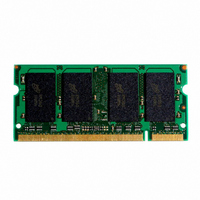
MT9VDDT6472PHY-40BF2 Micron Technology Inc, MT9VDDT6472PHY-40BF2 Datasheet - Page 14

MT9VDDT6472PHY-40BF2
Manufacturer Part Number
MT9VDDT6472PHY-40BF2
Description
MODULE DDR SDRAM 512MB 200SODIMM
Manufacturer
Micron Technology Inc
Datasheet
1.MT9VDDT1672PHG-335D2.pdf
(33 pages)
Specifications of MT9VDDT6472PHY-40BF2
Memory Type
DDR SDRAM
Memory Size
512MB
Speed
400MT/s
Package / Case
200-SODIMM
Lead Free Status / RoHS Status
Contains lead / RoHS non-compliant
Table 13: I
DDR SDRAM components only;
Notes: 1–5, 8, 10, 12, 47; notes appear on pages 19–22; 0°C
pdf: 09005aef808ffe58, source: 09005aef808ffdc7
DD9C16_32_64_128x72PHG.fm - Rev. B 9/04 EN
PARAMETER/CONDITION
OPERATING CURRENT: One device bank; Active-Precharge;
t
changing once per clock cyle; Address and control inputs
changing once every two clock cycles
OPERATING CURRENT: One device bank; Active-Read-
Precharge; Burst = 4
I
clock cycle
PRECHARGE POWER-DOWN STANDBY CURRENT: All device
banks idle; Power-down mode;
CKE = (LOW)
IDLE STANDBY CURRENT: CS# = HIGH; All device banks idle;
t
changing once per clock cycle. V
DM
ACTIVE POWER-DOWN STANDBY CURRENT: One device
bank active; Power-down mode;
CKE = LOW
ACTIVE STANDBY CURRENT: CS# = HIGH; CKE = HIGH; One
device bank; Active-Precharge;
(MIN); DQ, DM and DQS inputs changing twice per clock
cycle; Address and other control inputs changing once per
clock cycle
OPERATING CURRENT: Burst = 2; Reads; Continuous burst;
One device bank active; Address and control inputs
changing once per clock cycle; CK =
OPERATING CURRENT: Burst = 2; Writes; Continuous burst;
One device bank active; Address and control inputs
changing once per clock cycle;
DQS inputs changing twice per clock cycle
AUTO REFRESH CURRENT
SELF REFRESH CURRENT: CKE
OPERATING CURRENT: Four bank interleaving READs (BL=4)
with auto precharge with,
Address and control inputs change only during Active READ,
or WRITE commands
RC =
OUT
CK =
= 0mA; Address and control inputs changing once per
t
t
CK MIN; CKE = HIGH; Address and other control inputs
RC (MIN);
DD
t
CK =
;
Specifications and Conditions – 256MB
t
RC =
t
CK (MIN); DQ, DM and DQS inputs
t
t
RC (MIN);
RC =
t
0.2V
CK =
t
t
RC = RAS (MAX);
IN
CK =
t
t
RC (MIN);
CK =
= V
t
t
CK (MIN); I
CK (MIN); DQ, DM, and
t
t
REF
CK =
CK (MIN);
t
128MB, 256MB, 512MB, 1GB (x72, ECC, PLL, SR)
CK (MIN);
for DQ, DQS, and
t
t
REFC =
REFC = 7.8125µs
t
t
CK (MIN);
CK =
OUT
t
t
t
CK =
CK (MIN);
RFC (MIN)
= 0mA
t
CK
14
T
A
SYMBOL
I
I
I
I
I
I
I
DD 4 W
DD 3 N
DD 5 A
I
I
DD 2 P
DD 3 P
DD 4 R
I
I
I
DD 2 F
DD 0
DD 1
DD 5
DD 6
DD 7
+70°C; V
200-PIN DDR SDRAM SODIMM
Micron Technology, Inc., reserves the right to change products or specifications without notice.
DD
1,125
1,530
1,575
1,400
2,295
3,645
-335
450
270
540
35
54
36
= V
DD
Q = +2.5V ±0.2V
MAX
1,125
1,440
1,350
1,200
2,115
3,150
-262
405
225
450
36
54
36
©2004 Micron Technology, Inc. All rights reserved.
-26A/
1,305
1,350
1,200
2,115
3,150
-265
960
405
225
450
36
54
36
UNITS
mA
mA
mA
mA
mA
mA
mA
mA
mA
mA
mA
mA
ADVANCE
NOTES
21, 28,
21, 28,
20, 41
20, 41
20, 41
20, 43
24, 43
20, 42
43
44
43
20
9


