MT8HTF6464HDY-667D3 Micron Technology Inc, MT8HTF6464HDY-667D3 Datasheet
MT8HTF6464HDY-667D3
Specifications of MT8HTF6464HDY-667D3


Related parts for MT8HTF6464HDY-667D3


MT8HTF6464HDY-667D3 Summary of contents
Page 1
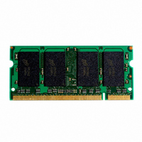
... DDR2 SDRAM SODIMM MT8HTF3264HDY – 256MB MT8HTF6464HDY – 512MB MT8HTF12864HDY – 1GB Features • 200-pin, small-outline dual in-line memory module (SODIMM) • Fast data transfer rates: PC2-3200, PC2-4200, PC2-5300, or PC2-6400 • 256MB (32 Meg x 64), 512MB (64 Meg x 64), or 1GB (128 Meg x 64) • ...
Page 2
... DDR2 SDRAM Module 2 Part Number Density MT8HTF6464HDY-80E__ MT8HTF6464HTY-80E__ MT8HTF6464HDY-800__ MT8HTF6464HTY-800__ MT8HTF6464HDY-667__ MT8HTF6464HTY-667__ MT8HTF6464HDY-53E__ MT8HTF6464HTY-53E__ MT8HTF6464HDY-40E__ MT8HTF6464HTY-40E__ PDF: 09005aef80ebed66 htf8c32_64_128x64hd.pdf - Rev. E 3/10 EN 256MB, 512MB, 1GB (x64, DR) 200-Pin DDR2 SODIMM 256MB 8K 8K A[12:0] 4 BA[1:0] 256Mb (16 Meg x 16) 512 A[8:0] 2 S#[1:0] Module ...
Page 3
... The data sheet for the base device can be found on Micron’s Web site. Notes: 2. All part numbers end with a two-place code (not shown) that designates component and PCB revisions. Consult factory for current revision codes. Example: MT8HTF6464HDY-667D3. PDF: 09005aef80ebed66 htf8c32_64_128x64hd.pdf - Rev. E 3/10 EN ...
Page 4
Pin Assignments and Descriptions Table 6: Pin Assignments 200-Pin DDR2 SODIMM Front Pin Symbol Pin Symbol Pin DQS2 101 REF 103 DQ0 55 DQ18 105 7 DQ1 57 DQ19 107 ...
Page 5
... Pin Descriptions The pin description table below is a comprehensive list of all possible pins for all DDR2 modules. All pins listed may not be supported on this module. See Pin Assignments for information specific to this module. Table 7: Pin Descriptions Symbol Type Ax Input BAx Input ...
Page 6
Table 7: Pin Descriptions (Continued) Symbol Type SDA I/O RDQSx, Output RDQS#x Err_Out# Output (open drain Supply DD DDQ V Supply DDSPD V Supply REF V Supply SS – NC – NF – NU – RFU PDF: 09005aef80ebed66 ...
Page 7
Functional Block Diagram Figure 2: Functional Block Diagram S1# S0# CS# UDQS DQS0 UDQS# DQS0# UDM DM0 DQ DQ0 DQ DQ1 DQ DQ2 DQ DQ3 DQ DQ4 DQ DQ5 DQ DQ6 U1 DQ DQ7 DQS1 LDQS DQS1# LDQS# DM1 LDM ...
Page 8
... DRAM core and eight corresponding n-bit-wide, one-half-clock-cycle data trans- fers at the I/O pins. DDR2 modules use two sets of differential signals: DQS, DQS# to capture data and CK and CK# to capture commands, addresses, and control signals. Differential clocks and data strobes ensure exceptional noise immunity for these signals and provide precise crossing points to capture input signals ...
Page 9
Electrical Specifications Stresses greater than those listed may cause permanent damage to the module. This is a stress rating only, and functional operation of the module at these or any other condi- tions outside those indicated in the device data ...
Page 10
... Design Considerations Simulations Micron memory modules are designed to optimize signal integrity through carefully de- signed terminations, controlled board impedances, routing topologies, trace length matching, and decoupling. However, good signal integrity starts at the system level. Mi- cron encourages designers to simulate the signal characteristics of the system's memo- ry bus to ensure adequate signal integrity of the entire memory system ...
Page 11
I Specifications DD Table 10: DDR2 I Specifications and Conditions – 256MB DD Values shown for MT47H16M16 DDR2 SDRAM only and are computed from values specified in the 256Mb (16 Meg x 16) component data sheet Parameter Operating one bank ...
Page 12
Table 10: DDR2 I Specifications and Conditions – 256MB (Continued) DD Values shown for MT47H16M16 DDR2 SDRAM only and are computed from values specified in the 256Mb (16 Meg x 16) component data sheet Parameter Operating bank interleave read current: ...
Page 13
Table 11: DDR2 I Specifications and Conditions – 512MB DD Values shown for MT47H32M16 DDR2 SDRAM only and are computed from values specified in the 512Mb (32 Meg x 16) component data sheet Parameter Operating one bank active-precharge current: t ...
Page 14
Table 11: DDR2 I Specifications and Conditions – 512MB (Continued) DD Values shown for MT47H32M16 DDR2 SDRAM only and are computed from values specified in the 512Mb (32 Meg x 16) component data sheet Parameter Operating bank interleave read current: ...
Page 15
Table 12: DDR2 I Specifications and Conditions – 1GB (Die Revision A) DD Values shown for MT47H64M16 DDR2 SDRAM only and are computed from values specified in the 1Gb (64 Meg x 16) com- ponent data sheet Parameter Operating one ...
Page 16
Table 13: DDR2 I Specifications and Conditions – 1GB (Die Revision E and G) DD Values shown for MT47H64M16 DDR2 SDRAM only and are computed from values specified in the 1Gb (64 Meg x 16) com- ponent data sheet Parameter ...
Page 17
Table 13: DDR2 I Specifications and Conditions – 1GB (Die Revision E and G) (Continued) DD Values shown for MT47H64M16 DDR2 SDRAM only and are computed from values specified in the 1Gb (64 Meg x 16) com- ponent data sheet ...
Page 18
Serial Presence-Detect For the latest SPD data, refer to Micron's SPD page: www.micron.com/SPD. Table 14: SPD EEPROM Operating Conditions Parameter/Condition Supply voltage Input high voltage: logic 1; All inputs Input low voltage: logic 0; All inputs Output low voltage: I ...
Page 19
Module Dimensions Figure 3: 200-Pin DDR2 SODIMM 2.0 (0.079) R (2X) U1 1.8 (0.071) (2X) 6.0 (0.236) TYP 2.0 (0.079) TYP U5 Pin 200 1. All dimensions are in millimeters (inches); MAX/MIN or typical (TYP) where noted. Notes: 2. The ...