PDSP2114 OSRAM Opto Semiconductors Inc, PDSP2114 Datasheet
PDSP2114
Specifications of PDSP2114


Related parts for PDSP2114


PDSP2114 Summary of contents
Page 1
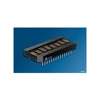
... High Efficiency Green PDSP2114 DESCRIPTION The PDSP2110 (Red), PDSP2111 (Yellow), PDSP2112 (Super-red), PDSP2113 (Green), and PDSP2114 (High Efficiency Green) are eight digit dot matrix, parallel input, alphanumeric Intelligent Display devices. The 5.10 mm (0.200’’) high digits are packaged in a rugged, high quality, optically transparent, 15.24 mm (0.6’ ...
Page 2
... PDSP2110, PDSP2111, PDSP2112, PDSP2113, PDSP2114 Ordering Information Type Color of Emission PDSP2110 red PDSP2111 yellow PDSP2112 super-red PDSP2113 green PDSP2114 high efficiency green Package Outlines EIA Date Part Number Code PDSP211X Z OSRAM 2.54 (0.100) typ. 4.79 (0.189) 42.67 (1.680) max. 5.34 (0.210) ...
Page 3
... PDSP2110, PDSP2111, PDSP2112, PDSP2113, PDSP2114 Maximum Ratings (T =25°C) A Parameter Operating temperature range Storage temperature range V DC Supply Voltage, to GND CC (max. voltage with no LEDs on) Input Voltage Levels Relative to GND Solder Temperature 1.59 mm (0.063“) below seating plane, t < 5.0 s Relative Humidity (non-condensing) Optical Characteristics at 25° ...
Page 4
... PDSP2110, PDSP2111, PDSP2112, PDSP2113, PDSP2114 Enlarged Character Font 2.85 (0.112 0.65 (0.026) typ. Data Wait Write control word - Wait 130 ns clear bit enabled Write Cycle Timing Diagram FL, A3-A0 CE Tces WR D7-D0 Notes: 1. All input voltages are V =0 These wave forms are not edge triggered. ...
Page 5
... PDSP2110, PDSP2111, PDSP2112, PDSP2113, PDSP2114 Electrical Characteristics at 25°C Parameters Limits Min. 4 Blank — digits — dots/character 1) 8 digits — dots/character I Current — IP (with pull-up) I, Input Leakage Current — (no pull-up) Input Voltage High 2 Input Voltage Low GND V IL –0.3 Output Voltage Low — ...
Page 6
... PDSP2110, PDSP2111, PDSP2112, PDSP2113, PDSP2114 Top View 28 Pins Digit 1 Pins Pin Assignments Pin Function Pin 1 RST Substr. bias Connect 19 11 CLKSEL 18 12 CLK I 2006-01-23 Pin Definitions 15 Pin Function 1 RST 7-9 Substr. bias Used to bias IC substrate, must be connected IDPA5116 10 No connect 11 CLKSEL ...
Page 7
... PDSP2110, PDSP2111, PDSP2112, PDSP2113, PDSP2114 Cascading the PDSP211X Displays RST Display D0-D7 A0-A4 Data I/O Address Address Decoder 2006-01- RST CLK CLK I/O SEL more displays in between CE Address Decode Chip RST CLK CLK I/O SEL Display D0-D7 A0-A4 CE IDCD5031 ...
Page 8
... PDSP2110, PDSP2111, PDSP2112, PDSP2113, PDSP2114 Character Set ROM Page 1 (D7 ASCII CODE HEX ROM Page 2 (D7= ASC|| CODE HEX 2006-01- IDCS5093 IDCS5094 ...
Page 9
... PDSP2110, PDSP2111, PDSP2112, PDSP2113, PDSP2114 Block Diagram RST CLK I/O OSC CLKSEL D7 D6 Display D5 Memory bits Address Lines Address Decoder Functional Description The PDSP211X block diagram is comprised of the following major blocks and registers. Display Memory consists bit RAM block. Each of the eight 8-bit words holds the 7-bit ASCII data (bit D0-D6) ...
Page 10
... PDSP2110, PDSP2111, PDSP2112, PDSP2113, PDSP2114 Data Input Commands Signals X=Don’t care Power up Sequence Upon power up display will come on at random. Thus the display should be reset on power-up. The reset will clear the Flash RAM, Control Word Register and reset the internal counter. All the dig- its will show blanks and display brightness level will be 100% ...
Page 11
... PDSP2110, PDSP2111, PDSP2112, PDSP2113, PDSP2114 Control Word Format Display Brightness The display can be programmed to vary between blank, 13%, 20%, 27%, 40%, 53%, 80% and full brightness. Bits D0, D1 and D2 control the display brightness X=Don’t Care Flash RAM Function Character Flash is controlled by FL pin, bit D0 and control word bit D3. Combination of FL being low, proper digit address and D0 being high will write a flash bit into the Flash RAM Register ...
Page 12
... PDSP2110, PDSP2111, PDSP2112, PDSP2113, PDSP2114 Clear Function Clear function will clear the display. The Flash RAM will be set to all zeros. An ASCII blank code (20H) will be written into the display memory. The user must wait 3 write a new control word to the display with control word bit disable clear before writing any data to the display memory, otherwise all new data to the display memory will remain cleared ...
Page 13
... PDSP2110, PDSP2111, PDSP2112, PDSP2113, PDSP2114 Electrical and Mechanical Considerations Voltage Transient Suppression For best results power the display and the components that inter- face with the display to avoid logic inputs higher than V tionally, the LEDs may cause transients in the power supply line while they change display states. The common practice is to place a parallel combination of a 0.01 µ ...
Page 14
... PDSP2110, PDSP2111, PDSP2112, PDSP2113, PDSP2114 Revision History: 2006-01-23 Previous Version: 2005-01-10 Page Subjects (major changes since last revision) all Lead free device ublished by P OSRAM Opto Semiconductors GmbH Wernerwerkstrasse 2, D-93049 Regensburg www.osram-os.com © All Rights Reserved. Attention please! The information describes the type of component and shall not be considered as assured characteristics. ...