PDSP2114 OSRAM Opto Semiconductors Inc, PDSP2114 Datasheet - Page 10
PDSP2114
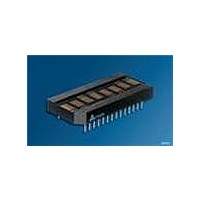
Manufacturer Part Number
PDSP2114
Description
DISPLAY PROG 8CHAR .200" 5X7 HEG
Manufacturer
OSRAM Opto Semiconductors Inc
Series
Alphanumeric Programmable Display™r
Datasheet
1.PDSP2110.pdf
(14 pages)
Specifications of PDSP2114
Millicandela Rating
510µcd
Size / Dimension
1.70" L x 0.77" W x 0.21" H (42.67mm x 19.58mm x 5.31mm)
Color
Green
Configuration
5 x 7
Number Of Digits
8
Character Size
0.2 in
Illumination Color
High Efficiency Green
Wavelength
568 nm
Maximum Operating Temperature
+ 85 C
Minimum Operating Temperature
- 40 C
Luminous Intensity
510 ucd
Viewing Area (w X H)
2.85 mm x 4.81 mm
Display Type
5 x 7 Dot Matrix
Emitting Color
Hi-Eff. Green
Digit Size (in)
.2in
Viewing Area Height (mm)
4.81mm
Package Type
Panel
Operating Supply Voltage (min)
4.5V
Operating Supply Voltage (typ)
5V
Operating Supply Voltage (max)
5.5V
Operating Temperature Classification
Industrial
Operating Temp Range
-40C to 85C
Mounting
Through Hole
Pin Count
28
Total Thickness (mm)
5.1mm
Opto Display Type
Panel
Pattern Type
Dot Matrix
Lead Free Status / RoHS Status
Lead free / RoHS Compliant
Voltage - Forward (vf) Typ
-
Internal Connection
-
Lead Free Status / Rohs Status
Compliant
Other names
Q68000A8533


Data Input Commands
Signals
Power up Sequence
Upon power up display will come on at random. Thus the display
should be reset on power-up. The reset will clear the Flash RAM,
Control Word Register and reset the internal counter. All the dig-
its will show blanks and display brightness level will be 100%.
2006-01-23
CE
1
X
0
0
0
0
0
0
0
0
0
0
0
0
0
0
0
0
0
X=Don’t care
0
WR
X
1
0
0
0
0
0
0
1
0
0
0
0
0
0
0
0
0
FL
X
X
1
1
1
1
1
1
1
1
1
0
0
0
0
0
0
0
0
A3
X
X
0
1
1
1
1
1
1
1
1
X
X
X
X
X
X
X
X
PDSP2110, PDSP2111, PDSP2112, PDSP2113, PDSP2114
A2
X
X
0
0
0
0
0
1
1
1
1
0
0
0
1
1
1
1
1
A1
X
X
0
0
0
1
1
0
0
0
1
0
0
1
1
0
0
1
1
X
X
0
0
1
0
1
0
1
0
1
A0
0
1
0
1
0
1
0
1
Operation
No operation
No operation
Write Control Register
Digit 0 (left)
Digit 1
Digit 2
Digit 3
Digit 4
Digit 5
Digit 6
Digit 7 (right)
Digit 0 (left)
Digit 1
Digit 2
Digit 3
Digit 4
Digit 5
Digit 6
Digit 7 (right)
10
Microprocessor Interface
The interface to a microprocessor is through the 8-bit data bus
(D0-D7), the 4-bit address bus (A0-A3) and control lines FL , CE
and WR.
To write data (ASCII/ Control Word) into the display CE should be
held low, address and data signals stable and WR should be
brought low.
The Control Word is decoded by the Control Word Decode Logic.
Each code has a different function. The code for display brightness
changes the duty cycle for the column drivers. The peak LED cur-
rent stays the same but the average LED current diminishes
depending on the intensity level.
The character Flash Enable causes 2.0 Hz coming out of the
counter to be ANDED with column drive signal and makes the col-
umn driver to cycle at 2.0 Hz. Thus the character flashes at 2.0 Hz.
The display Blink works the same way as the Flash Enable but
causes all twenty column drivers to cycle at 2.0 Hz thereby making
all eight digits to blink at 2.0 Hz.
The Lamp Test causes the column drivers to run at 1/2 duty cycle
thus all the LEDs in all eight digits turn on at 50% intensity.
Clear bit clears the character RAM and writes a blank into the dis-
play memory. It however does not clear the control word.
ASCII Data or Control Word Data can be written into the display at
this point. For multiple display operation, CLK I/O must be properly
selected. CLK I/O will output the internal clock if CLKSEL=1, or will
allow input from an external clock if CLKSEL=0.
Write display data to
user RAM and Page
Select Register
D0–D6=ASCII Data
D7=0 Select ROM 1
D7=1 Select ROM 2
Write Flash RAM Register
D0=0 Flashing Charac. off
D0=1 Flashing Charac. on
D1–D7=X
Related parts for PDSP2114
Image
Part Number
Description
Manufacturer
Datasheet
Request
R

Part Number:
Description:
INTELLIGENT DISP 4CHAR 5X7 HERED
Manufacturer:
OSRAM Opto Semiconductors Inc
Datasheet:

Part Number:
Description:
DISPLAY 8DIGIT CERAMIC GREEN
Manufacturer:
OSRAM Opto Semiconductors Inc
Datasheet:

Part Number:
Description:
EMITTER IR 950NM 5MM SMD RADIAL
Manufacturer:
OSRAM Opto Semiconductors Inc
Datasheet:

Part Number:
Description:
LED TOPLED GREEN 570NM 2-PLCC
Manufacturer:
OSRAM Opto Semiconductors Inc
Datasheet:

Part Number:
Description:
INTERRUPTER RELFECT W/FILTR SMD
Manufacturer:
OSRAM Opto Semiconductors Inc
Datasheet:

Part Number:
Description:
LED Displays 5x7 Green 0.145 , 4-CHARACTER
Manufacturer:
OSRAM Opto Semiconductors Inc
Datasheet:

Part Number:
Description:
Q65110A4321_SIDELED PURE GREEN EOL150407
Manufacturer:
OSRAM Opto Semiconductors Inc
Datasheet:
Part Number:
Description:
Q65110A1202_RO DETECTOR 3/5MM_TR_RO
Manufacturer:
OSRAM Opto Semiconductors Inc
Datasheet:

Part Number:
Description:
PHOTODIODE 900NM 3MM W/FILTER
Manufacturer:
OSRAM Opto Semiconductors Inc
Datasheet:
Part Number:
Description:
INTELLIGENT DISP 4CHAR 5X7 HERED
Manufacturer:
OSRAM Opto Semiconductors Inc
Datasheet:
Part Number:
Description:
LED TOPLED GREEN 570NM 2-PLCC
Manufacturer:
OSRAM Opto Semiconductors Inc
Datasheet:
Part Number:
Description:
PHOTODIODE 900NM 3MM W/FILTER
Manufacturer:
OSRAM Opto Semiconductors Inc
Datasheet:

Part Number:
Description:
PHOTODIODE 850NM THRU-HOLE
Manufacturer:
OSRAM Opto Semiconductors Inc
Datasheet:

Part Number:
Description:
PHOTODIODE 880NM W/FILTER SMD
Manufacturer:
OSRAM Opto Semiconductors Inc
Datasheet: