PDSP2114 OSRAM Opto Semiconductors Inc, PDSP2114 Datasheet - Page 4
PDSP2114
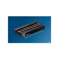
Manufacturer Part Number
PDSP2114
Description
DISPLAY PROG 8CHAR .200" 5X7 HEG
Manufacturer
OSRAM Opto Semiconductors Inc
Series
Alphanumeric Programmable Display™r
Datasheet
1.PDSP2110.pdf
(14 pages)
Specifications of PDSP2114
Millicandela Rating
510µcd
Size / Dimension
1.70" L x 0.77" W x 0.21" H (42.67mm x 19.58mm x 5.31mm)
Color
Green
Configuration
5 x 7
Number Of Digits
8
Character Size
0.2 in
Illumination Color
High Efficiency Green
Wavelength
568 nm
Maximum Operating Temperature
+ 85 C
Minimum Operating Temperature
- 40 C
Luminous Intensity
510 ucd
Viewing Area (w X H)
2.85 mm x 4.81 mm
Display Type
5 x 7 Dot Matrix
Emitting Color
Hi-Eff. Green
Digit Size (in)
.2in
Viewing Area Height (mm)
4.81mm
Package Type
Panel
Operating Supply Voltage (min)
4.5V
Operating Supply Voltage (typ)
5V
Operating Supply Voltage (max)
5.5V
Operating Temperature Classification
Industrial
Operating Temp Range
-40C to 85C
Mounting
Through Hole
Pin Count
28
Total Thickness (mm)
5.1mm
Opto Display Type
Panel
Pattern Type
Dot Matrix
Lead Free Status / RoHS Status
Lead free / RoHS Compliant
Voltage - Forward (vf) Typ
-
Internal Connection
-
Lead Free Status / Rohs Status
Compliant
Other names
Q68000A8533


Enlarged Character Font
Write Cycle Timing Diagram
Notes:
1. All input voltages are V
2. These wave forms are not edge triggered.
3. T
2006-01-23
Write control word -
clear bit enabled
bw
=T
as
Data
+T
ah
FL, A3-A0
0.65 (0.026) typ.
C1 C2
CE
WR
D7-D0
Wait 130 ns
2.85 (0.112)
IL
=0.8 V, V
Wait
C3
Tces
PDSP2110, PDSP2111, PDSP2112, PDSP2113, PDSP2114
C4
IH
=2.0 V.
C5
Dimensions in inch (mm)
Tas
Write control word -
clear bit enabled
R1
R2
R3
R4
R5
R6
R7
IDOD5202
Data
Tacc
Tw
IDTC5054
Tds
4
Tdh
Tah
Switching Specifications
(over operating temperature range and V
Symbol
T
T
T
T
T
T
T
T
T
T
T
Notes:
1)
2)
3)
acc
as
ces
ah
ceh
w
rc
clr
bw
ds
dh
(1)
(3 )
Tceh
Wait 300 ns min. after the reset function is turned off.
T
The Clear Cycle Time may be shortened by writing a second
Control Word with the Clear Bit disabled, 160 ns after the first
control word that enabled the Clear Bit.
The Flash RAM and Character RAM may not be accessed
until the Clear Cycle is complete.
(2)
Tbw
acc
=T
as
+T
Description
Time Between Writes
Display Access Time
Address Setup Time
Chip Enable Setup Time
Address Hold Time
Chip Enable Hold Time
Write Active Time
Data Valid Prior to Rising Edge
of Write
Data Hold Time
Reset Active Time
Clear Cycle Time
w
+T
ah
see Notes
see Notes
see Notes
see Notes
CC
=4.5 V)
Min.
30
130
10
0
20
0
100
50
20
300
3.0
Units
ns
ns
ns
ns
ns
ns
ns
ns
ns
ns
µs
Related parts for PDSP2114
Image
Part Number
Description
Manufacturer
Datasheet
Request
R

Part Number:
Description:
INTELLIGENT DISP 4CHAR 5X7 HERED
Manufacturer:
OSRAM Opto Semiconductors Inc
Datasheet:

Part Number:
Description:
DISPLAY 8DIGIT CERAMIC GREEN
Manufacturer:
OSRAM Opto Semiconductors Inc
Datasheet:

Part Number:
Description:
EMITTER IR 950NM 5MM SMD RADIAL
Manufacturer:
OSRAM Opto Semiconductors Inc
Datasheet:

Part Number:
Description:
LED TOPLED GREEN 570NM 2-PLCC
Manufacturer:
OSRAM Opto Semiconductors Inc
Datasheet:

Part Number:
Description:
INTERRUPTER RELFECT W/FILTR SMD
Manufacturer:
OSRAM Opto Semiconductors Inc
Datasheet:

Part Number:
Description:
LED Displays 5x7 Green 0.145 , 4-CHARACTER
Manufacturer:
OSRAM Opto Semiconductors Inc
Datasheet:

Part Number:
Description:
Q65110A4321_SIDELED PURE GREEN EOL150407
Manufacturer:
OSRAM Opto Semiconductors Inc
Datasheet:
Part Number:
Description:
Q65110A1202_RO DETECTOR 3/5MM_TR_RO
Manufacturer:
OSRAM Opto Semiconductors Inc
Datasheet:

Part Number:
Description:
PHOTODIODE 900NM 3MM W/FILTER
Manufacturer:
OSRAM Opto Semiconductors Inc
Datasheet:
Part Number:
Description:
INTELLIGENT DISP 4CHAR 5X7 HERED
Manufacturer:
OSRAM Opto Semiconductors Inc
Datasheet:
Part Number:
Description:
LED TOPLED GREEN 570NM 2-PLCC
Manufacturer:
OSRAM Opto Semiconductors Inc
Datasheet:
Part Number:
Description:
PHOTODIODE 900NM 3MM W/FILTER
Manufacturer:
OSRAM Opto Semiconductors Inc
Datasheet:

Part Number:
Description:
PHOTODIODE 850NM THRU-HOLE
Manufacturer:
OSRAM Opto Semiconductors Inc
Datasheet:

Part Number:
Description:
PHOTODIODE 880NM W/FILTER SMD
Manufacturer:
OSRAM Opto Semiconductors Inc
Datasheet: