HFBR-2119TZ Avago Technologies US Inc., HFBR-2119TZ Datasheet - Page 11
HFBR-2119TZ
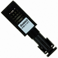
Manufacturer Part Number
HFBR-2119TZ
Description
RECEIVER FIBER OPTIC ST 266MBD
Manufacturer
Avago Technologies US Inc.
Datasheet
1.HFBR-2119TZ.pdf
(12 pages)
Specifications of HFBR-2119TZ
Voltage - Supply
4.5 V ~ 5.5 V
Power - Minimum Receivable
-28dBm
Current - Supply
185mA
Applications
General Purpose
Function
Fiber Channel applications or for general purpose fiber optic data link transmission
Product
Receiver
Data Rate
266 MBd
Wavelength
1380 nm (Max)
Maximum Rise Time
2.2 ns
Maximum Fall Time
2.2 ns
Pulse Width Distortion
0.97 ns
Maximum Output Current
50 mA
Operating Supply Voltage
4.5 V to 5.5 V
Maximum Operating Temperature
+ 70 C
Minimum Operating Temperature
0 C
Package / Case
DIP With Connector
Lead Free Status / RoHS Status
Lead free / RoHS Compliant
For Use With
Multimode Glass
Lead Free Status / RoHS Status
Lead free / RoHS Compliant, Lead free / RoHS Compliant
Other names
516-2051
Available stocks
Company
Part Number
Manufacturer
Quantity
Price
Company:

Part Number:
HFBR-2119TZ
Manufacturer:
Avago Technologies US Inc.
Quantity:
135


Notes:
11
1. This is the maximum voltage that can be
2. When component testing these products,
3. The outputs are terminated with 50
4. The power supply current needed to
5. These optical power values are measured
6. The Extinction Ratio is a measure of the
7. This parameter complies with the
applied across the Differential Transmitter
Data Inputs to prevent damage to the
input ESD protection circuit.
do not short the receiver Data or Signal
Detect outputs directly to ground to avoid
damage to the part.
connected to V
operate the transmitter is provided to
differential ECL circuitry. This circuitry
maintains a nearly constant current flow
from the power supply. Constant current
operation helps to prevent unwanted
electrical noise from being generated and
conducted or emitted to neighboring
circuitry.
as follows:
• The Beginning of Life (BOL) to the End
• Over the specified operating voltage and
• With 25 MBd (12.5 MHz square-wave),
• At the end of one meter of noted optical
The average power value can be
converted to a peak power value by adding
3 dB. Higher output optical power
transmitters are available on special
request.
modulation depth of the optical signal.
The data “0” output optical power is
compared to the data “1” peak output
optical power and expressed as a
percentage. With the transmitter driven by
a 12.5 MHz square-wave signal, the
average optical power is measured. The
data “1” peak power is then calculated by
adding 3 dB to the measured average
optical power. The data “0” output optical
power is found by measuring the optical
power when the transmitter is driven by a
logic “0” input. The extinction ratio is the
ratio of the optical power at the “0” level
compared to the optical power at the “1”
level expressed as a percentage or in
decibels.
requirements for the tradeoffs between
center wave length, spectral width, and
rise/fall times shown in Figure 8.
of Life (EOL) optical power degradation
is typically 1.5 dB per the industry
convention for long wavelength LEDs.
The actual degradation observed in
Avago Technologies’s 1300 nm LED
products is < 1dB, as specified in this
data sheet.
temperature ranges.
input signal.
fiber with cladding modes removed.
CC
- 2 V.
10. Random Jitter is specified with a
11. This specification is intended to indicate
12. All conditions of Note 11 apply except that
13. This value is measured during the
8. The optical rise and fall times are measured
9. Deterministic Jitter is defined as the
from 10% to 90% when the transmitter is
driven by a 25 MBd (12.5 MHz square-
wave) input signal. This parameter
complies with the requirements for the
tradeoffs between center wavelength,
spectral width, and rise/fall times shown
in Figure 8.
combination of Duty Cycle Distortion and
Data Dependent Jitter. Deterministic
Jitter is measured with a test pattern
consisting of repeating K28.5
(00111110101100000101) data bytes and
evaluated per the method in FC-PH Annex
A.4.3.
sequence of K28.7 (square wave of
alternating 5 ones and 5 zeros) data bytes
and, for the receiver, evaluated at a Bit-
Error-Ratio (BER) of 1 x 10
method in FC-PH Annex A.4.4.
the performance of the receiver when
Input Optical Power signal characteristics
are present per the following definitions.
The Input Optical Power dynamic range
from the minimum level (with a window
time-width) to the maximum level is the
range over which the receiver is
guaranteed to provide output data with a
Bit-Error-Ratio (BER) better than or equal
to 1 x 10
• At the Beginning of Life (BOL).
• Over the specified operation
• Input symbol pattern is a 266 MBd,
• Receiver data window time-width is
• The maximum total jitter added by the
the measurement is made at the center of
the symbol with no window time-width.
transition from low to high levels of input
optical power.
temperature and voltage ranges.
2
pattern.
mid-symbol. This data window time
width is calculated to simulate the
effect of worst-case input jitter per FC-
PH Annex J and clock recovery sampling
position in order to insure good
operation with the various FC-0 receiver
circuits.
receiver and the maximum total jitter
presented to the clock recovery circuit
comply with the maximum limits listed
in Annex J, but the allocations of the Rx
added jitter between deterministic jitter
and random jitter are different than in
Annex J.
7
0.94 ns or greater and centered at
- 1 pseudo-random bit stream data
-12
.
-12
per the
14. This value is measured during the
15. These values are measured with the
16. The power dissipation value is the power
17. These values are measured with respect
18. The output rise and fall times are
19. The Signal Detect output shall be
20. Signal Detect output shall be de-asserted,
21. This value is measured with an output
transition from high to low levels of input
optical power.
outputs terminated into 50
to V
level of -14 dBm average.
dissipated in the transmitter or the
receiver itself. Power dissipation is
calculated as the sum of the products of
supply voltage and supply current, minus
the sum of the products of the output
voltages and currents.
to V
50
measured between 20% and 80% levels
with the output connected to V
through 50 .
asserted, logic-high (V
after a step increase of the Input Optical
Power.
logic-low (V
decrease in the Input Optical Power.
load R
CC
CC
connected to V
L
with the output terminated into
- 2 V and an input optical power
= 10 k .
OL
), within 350 s after a step
CC
OH
- 2 V.
), within 100 s
connected
CC
- 2 V
Related parts for HFBR-2119TZ
Image
Part Number
Description
Manufacturer
Datasheet
Request
R

Part Number:
Description:
FIBER OPTIC CONN LATCH GRY SIMPL
Manufacturer:
Avago Technologies US Inc.
Datasheet:

Part Number:
Description:
FIBER OPTIC CONN LATCH BLU SIMPL
Manufacturer:
Avago Technologies US Inc.
Datasheet:

Part Number:
Description:
FIBER OPTIC CRIMPLESS CONN GRAY
Manufacturer:
Avago Technologies US Inc.
Datasheet:

Part Number:
Description:
FIBER OPTIC CONN BLUE SIMPLEX
Manufacturer:
Avago Technologies US Inc.
Datasheet:

Part Number:
Description:
FIBER OPTIC CONN LATCH DUPLEX
Manufacturer:
Avago Technologies US Inc.
Datasheet:

Part Number:
Description:
FIBER OPTIC CONN DUPLEX
Manufacturer:
Avago Technologies US Inc.
Datasheet:

Part Number:
Description:
FIBER OPTIC CONN GRAY SIMPLEX
Manufacturer:
Avago Technologies US Inc.
Datasheet:

Part Number:
Description:
FIBER OPTIC CBL DUPLEX 1=100M
Manufacturer:
Avago Technologies US Inc.
Datasheet:

Part Number:
Description:
FIBER OPTIC CBL DUPLEX 1=500M
Manufacturer:
Avago Technologies US Inc.
Datasheet:

Part Number:
Description:
FIBER OPTIC CBL CONN DUPLEX 5M
Manufacturer:
Avago Technologies US Inc.
Datasheet:

Part Number:
Description:
OPTOCOUPLER GATE DRV 2A 16-SOIC
Manufacturer:
Avago Technologies US Inc.
Datasheet:
Part Number:
Description:
OPTOCOUPLER 2CH 2.5A 16-SOIC
Manufacturer:
Avago Technologies US Inc.
Datasheet:

Part Number:
Description:
OPTOCOUPLER GATE DRV 0.4A 16SOIC
Manufacturer:
Avago Technologies US Inc.
Datasheet:

Part Number:
Description:
OPTOCOUPLER 2.0A 250KHZ 8-DIP
Manufacturer:
Avago Technologies US Inc.
Datasheet:

Part Number:
Description:
OPTOCOUPLER 2.0A 250KHZ GW 8-SMD
Manufacturer:
Avago Technologies US Inc.
Datasheet: