AFBR-5803Z Avago Technologies US Inc., AFBR-5803Z Datasheet - Page 12
AFBR-5803Z
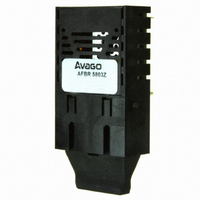
Manufacturer Part Number
AFBR-5803Z
Description
TXRX OPT 1X9 100MBPS DUPLEX SC
Manufacturer
Avago Technologies US Inc.
Datasheet
1.AFBR-5803ATZ.pdf
(16 pages)
Specifications of AFBR-5803Z
Data Rate
100Mbps
Wavelength
1300nm
Applications
General Purpose
Voltage - Supply
3.3V, 5V
Connector Type
SC
Mounting Type
Through Hole
Function
Implement FDDI and ATM at the 100 Mbps/125 MBd rate
Product
Transceiver
Pulse Width Distortion
0.69 ns (Max)/2.14 ns (Max)
Maximum Output Current
50 mA
Operating Supply Voltage
4.75 V to 5.25 V
Maximum Operating Temperature
+ 70 C
Minimum Operating Temperature
0 C
Lead Free Status / RoHS Status
Lead free / RoHS Compliant
For Use With
Multimode Glass
Lead Free Status / RoHS Status
Lead free / RoHS Compliant, Lead free / RoHS Compliant
Other names
516-1991


Absolute Maximum Ratings
Stresses in excess of the absolute maximum ratings can cause catastrophic damage to the device. Limits apply to each parameter
in isolation, all other parameters having values within the recommended operating conditions. It should not be assumed that
limiting values of more than one parameter can be applied to the product at the same time. Exposure to the absolute maximum
ratings for extended periods can adversely affect device reliability.
Recommended Operating Conditions
Notes:
A. Ambient Operating Temperature corresponds to transceiver case temperature of 0°C mininum to +85 °C maximum with necessary airflow ap-
B. Ambient Operating Temperature corresponds to transceiver case temperature of -10 °C mininum to +100 °C maximum with necessary airflow
Transmitter Electrical Characteristics
(AFBR-5803Z/5803TZ: T
(AFBR-5803AZ/AFBR-5803ATZ: T
1
Parameter
Storage Temperature
Lead Soldering Temperature
Lead Soldering Time
Supply Voltage
Data Input Voltage
Differential Input Voltage
Output Current
Parameter
Ambient Operating Temperature
AFBR-5803Z/5803TZ
AFBR-5803AZ/5803ATZ
Supply Voltage
Data Input Voltage - Low
Data Input Voltage - High
Data and Signal Detect Output Load
Parameter
Power Dissipation
plied. Recommended case temperature measurement point can be found in Figure 2.
applied. Recommended case temperature measurement point can be found in Figure 2.
Data Input Current - High
Data Input Current - Low
Supply Current
A
at V
at V
= 0°C to +70°C, V
CC
CC
= 3.3 V
= 5.0 V
A
= -10°C to +85°C, V
CC
Symbol
T
T
t
V
V
V
I
Symbol
T
T
V
V
V
V
R
Symbol
I
P
P
I
I
O
CC
IL
IH
SOLD
A
A
S
SOLD
CC
I
D
CC
CC
IL
IH
L
DISS
DISS
= 3.135 V to 3.5 V or 4.75 V to 5.25 V)
- V
- V
CC
CC
CC
Min.
-40
-0.5
-0.5
Min.
0
-10
3.135
4.75
-1.810
-1.165
Min.
= 3.135 V to 3.5 V or 4.75 V to 5.25 V)
-350
Typ.
Typ.
50
Typ.
0.45
0.76
133
18
-2
Max.
+100
+260
10
7.0
V
1.4
50
Max.
+70
+85
3.5
5.25
-1.475
-0.880
Max.
CC
0.97
175
350
0.6
Unit
°C
°C
sec.
V
V
V
mA
Unit
°C
°C
V
V
V
V
W
Unit
mA
µA
µA
W
W
Reference
Note 1
Reference
Note A
Note B
Note 2
Reference
Note 3
Related parts for AFBR-5803Z
Image
Part Number
Description
Manufacturer
Datasheet
Request
R

Part Number:
Description:
650nm FE Transceiver Eval Kit
Manufacturer:
Avago Technologies US Inc.
Datasheet:

Part Number:
Description:
TXRX OPT OC3 MTRJ SFF 2X5DIP
Manufacturer:
Avago Technologies US Inc.
Datasheet:

Part Number:
Description:
TXRX ETHERNET 125MBD MMF 2X5
Manufacturer:
Avago Technologies US Inc.
Datasheet:

Part Number:
Description:
TXRX OPT SFP DGTL 850NM IND
Manufacturer:
Avago Technologies US Inc.
Datasheet:

Part Number:
Description:
TXRX OPT SFF 4/2/1GBD 2X7
Manufacturer:
Avago Technologies US Inc.
Datasheet:

Part Number:
Description:
TXRX OPT SFP 4/2/1GBD 850NM
Manufacturer:
Avago Technologies US Inc.
Datasheet:

Part Number:
Description:
TXRX OPT XFP 10GB/S 850NM
Manufacturer:
Avago Technologies US Inc.
Datasheet:

Part Number:
Description:
TXRX OPT 1X9 100MBPS ST EXT TEMP
Manufacturer:
Avago Technologies US Inc.
Datasheet:

Part Number:
Description:
TXRX OPT 1X9 100MBPS SC EXT TEMP
Manufacturer:
Avago Technologies US Inc.
Datasheet:

Part Number:
Description:
TXRX OPT 1X9 100MBPS DUPLEX ST
Manufacturer:
Avago Technologies US Inc.
Datasheet:

Part Number:
Description:
OPTOCOUPLER GATE DRV 2A 16-SOIC
Manufacturer:
Avago Technologies US Inc.
Datasheet:
Part Number:
Description:
OPTOCOUPLER 2CH 2.5A 16-SOIC
Manufacturer:
Avago Technologies US Inc.
Datasheet:

Part Number:
Description:
OPTOCOUPLER GATE DRV 0.4A 16SOIC
Manufacturer:
Avago Technologies US Inc.
Datasheet:

Part Number:
Description:
OPTOCOUPLER 2.0A 250KHZ 8-DIP
Manufacturer:
Avago Technologies US Inc.
Datasheet:

Part Number:
Description:
OPTOCOUPLER 2.0A 250KHZ GW 8-SMD
Manufacturer:
Avago Technologies US Inc.
Datasheet: