AFBR-5930Z Avago Technologies US Inc., AFBR-5930Z Datasheet - Page 13
AFBR-5930Z
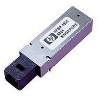
Manufacturer Part Number
AFBR-5930Z
Description
TXRX SBCON 200MBD 2X5 DIP
Manufacturer
Avago Technologies US Inc.
Datasheet
1.AFBR-5930Z.pdf
(14 pages)
Specifications of AFBR-5930Z
Applications
General Purpose
Data Rate
200MBd
Wavelength
1300nm
Voltage - Supply
3.135 V ~ 3.465 V
Connector Type
MTRJ
Mounting Type
Through Hole
Data Rate Max
0.2Gbps
Supply Voltage
3.3V
Wavelength Typ
1300nm
Leaded Process Compatible
Yes
Lead Free Status / RoHS Status
Lead free / RoHS Compliant


Notes:
1.
2.
3.
.
5.
.
.
8.
9.
10. From an assumed Gaussian-shaped wavelength distribution, the relationship between FWHM and RMS values for Spectral Width is 2.35 x RMS =
11. Input conditions: 100 MHz, square wave signal, input voltages are in the range specified for V
12. Measured with electrical input signal rise and fall time of 0.35 to 1.3 ns (20-80%) at the transmitter input pins. Optical output rise and fall times are
13. Transmitter Systematic Jitter is equal to the sum of Duty Cycle Distortion (DCD) and Data Dependent Jitter (DDJ). DCD is equivalent to Pulse-Width
1. This specification is intended to indicate the performance of the receiver section of the transceiver when Input Optical Power signal characteristics
15. All conditions of note 1 apply except that the measurement is made at the center of the symbol with no window time-width.
1. The receiver systematic jitter specification applies to optical powers between –1.5 dBm avg. to –2.0 dBm avg. at the receiver. Receiver Systematic
1. Eye-width specified defines the minimum clock time-position range, centered around the center of the 5 ns baud interval, at which the BER must
18. Status Flag switching thresholds:
19. Status Flag Hysteresis is the difference in low-to-high and high-to-low switching thresholds. Thresholds must lie within optical power limits speci-
20. The Status Flag output shall be asserted within 500 µs after a step increase of the Input Optical Power.
21. S t at u s Fl a g o u t p u t s h a l l b e d e - a s s e r te d w i t h i n 5 0 0 µ s a f te r a s te p d e c re a s e i n t h e I n p u t O p t i c a l Powe r.
This is the maximum voltage that can be applied across the Differential Transmitter Data Inputs to prevent damage to the input ESD protection
circuit.
The outputs are terminated with 50 W connected to V
The power supply current needed to operate the transmitter is provided to differential ECL circuitry. This circuitry maintains a nearly constant
current flow from the power supply. Constant current operation helps to prevent unwanted electrical noise from being generated and conducted
or emitted to neighboring circuitry.
The power dissipation value is the power dissipated in the receiver itself. Power dissipation is calculated as the sum of the products of supply
voltage and currents, minus the sum of the products of the output voltages and currents.
This value is measured with the outputs terminated into 50 W connected to V
This value is measured with respect to V
The output rise time and fall times are measured between 20% and 80% levels with the output connected to V
These optical power values are measured with the following conditions:
• The Beginning of Life (BOL) to theEnd of Life (EOL) optical power degradation is assumed to be 1.5 dB per the industry convention for long wave-
length LEDs. The actual degradation observed in normal commercial environments will be <1.0 dB with Avago Technologies 1300 nm LED products.
• Over the specified operating voltage and temperature ranges.
• Input Signal: 1010 data pattern, 200 Mb/s NRZ code.
The Extinction Ratio is a measure of the modulation depth of the optical signal. The data “0” output optical power is compared to the data “1” peak
output optical and expressed in decibels. With the transmitter driven by a HALT Line State (12.5 Mhz square-wave) signal, the average optical
power is measured. The data “1” peak power is then calculated by adding 3 dB to the measured average optical power. The data “0” output optical
power is found by measuring the optical power when the transmitter is driven by a logic “0” input. The Extinction Ratio is the ratio of the optical
power at the “0” level compared to the optical power at the “1” level expressed in decibels.
FWHM.
measured between 20% and 80% levels.
Distortion (PWD). Systematic Jitter is measured at the 50% signal level with 200 MBd, PRBS 2
are present per the following conditions. The Input Optical Power dynamic range from the minimum level (with a window time-width) to the
maximum level is the range over which the receiver is guaranteed to provide output data with a Bit Error Ratio (BER) better than or equal to 10
• At the Beginning of Life (BOL).
• Over the specified operatingtemperature and voltage ranges.
• Receiver data window time-width is 1. ns or greater and centered at mid-symbol.
• Input signal is 200 MBd, Pseudo Random-Bit-Stream 2
• Transmitter cross-talk effects have been included in Receiver sensitivity. Transmitter should be running at 50% duty cycle (nominal) between
8 - 200 Mb/s, while Receiver sensitivity is measured.
Jitter is equal to the sum of Duty Cycle Distortion (DCD) and Data Dependent Jitter (DDJ). DCD is equivalent to Pulse-Width Distortion (PWD).
Systematic Jitter is measured at the 50% signal level with 200 MBd, PRBS 2
be 10
than 1.0 dB.
Direction of decreasing optical power:
If Power >–3.0 dBm avg., then SF = 1 (high)
If Power <–5.0 dBm avg., then SF = 0 (low)
Direction of increasing optical power:
If Power >–35.5 dBm avg., then SF = 1 (high)
fied. The Hysteresis is desired to avoid Status Flag chatter when the optical input is near the threshold.
The step will be from a low Input Optical Power <–5.5 dBm avg., to >–35.5 dBm avg.
The Step will be from a high Input Optical Power >–3.0 dBm avg. to <–5.0 dBm avg.
If Power <–5.5 dBm avg., then SF = 0 (low)
–12
or better. Test data pattern is PRBS 2
CC
with the output terminated into 50 W connected to V
–1. The typical change in input optical power to open the eye to 1. nsec from a closed eye is less
CC
–2 V.
–1 data pattern.
–1 electrical output data pattern.
CC
–2 V and an Input Optical Power Level of –1.5 dBm average.
IL
–1 electrical input data pattern.
and V
CC
–2 V.
IH .
CC
– 2 V through 50 W.
–15
.
Related parts for AFBR-5930Z
Image
Part Number
Description
Manufacturer
Datasheet
Request
R

Part Number:
Description:
650nm FE Transceiver Eval Kit
Manufacturer:
Avago Technologies US Inc.
Datasheet:

Part Number:
Description:
TXRX OPT OC3 MTRJ SFF 2X5DIP
Manufacturer:
Avago Technologies US Inc.
Datasheet:

Part Number:
Description:
TXRX ETHERNET 125MBD MMF 2X5
Manufacturer:
Avago Technologies US Inc.
Datasheet:

Part Number:
Description:
TXRX OPT SFP DGTL 850NM IND
Manufacturer:
Avago Technologies US Inc.
Datasheet:

Part Number:
Description:
TXRX OPT SFF 4/2/1GBD 2X7
Manufacturer:
Avago Technologies US Inc.
Datasheet:

Part Number:
Description:
TXRX OPT SFP 4/2/1GBD 850NM
Manufacturer:
Avago Technologies US Inc.
Datasheet:

Part Number:
Description:
TXRX OPT XFP 10GB/S 850NM
Manufacturer:
Avago Technologies US Inc.
Datasheet:

Part Number:
Description:
TXRX OPT 1X9 100MBPS ST EXT TEMP
Manufacturer:
Avago Technologies US Inc.
Datasheet:

Part Number:
Description:
TXRX OPT 1X9 100MBPS SC EXT TEMP
Manufacturer:
Avago Technologies US Inc.
Datasheet:

Part Number:
Description:
TXRX OPT 1X9 100MBPS DUPLEX SC
Manufacturer:
Avago Technologies US Inc.
Datasheet:

Part Number:
Description:
OPTOCOUPLER GATE DRV 2A 16-SOIC
Manufacturer:
Avago Technologies US Inc.
Datasheet:
Part Number:
Description:
OPTOCOUPLER 2CH 2.5A 16-SOIC
Manufacturer:
Avago Technologies US Inc.
Datasheet:

Part Number:
Description:
OPTOCOUPLER GATE DRV 0.4A 16SOIC
Manufacturer:
Avago Technologies US Inc.
Datasheet:

Part Number:
Description:
OPTOCOUPLER 2.0A 250KHZ 8-DIP
Manufacturer:
Avago Technologies US Inc.
Datasheet:

Part Number:
Description:
OPTOCOUPLER 2.0A 250KHZ GW 8-SMD
Manufacturer:
Avago Technologies US Inc.
Datasheet: