AFBR-53D3Z Avago Technologies US Inc., AFBR-53D3Z Datasheet
AFBR-53D3Z
Specifications of AFBR-53D3Z


Related parts for AFBR-53D3Z


AFBR-53D3Z Summary of contents
Page 1
... This singleended PECL output is designed to drive a standard PECL input through a 50 Ω PECL load. Features • • • • • AFBR-53D3 is Compliant with ANSI X3.297-1996 Fibre Channel Physical Interface FC-PH-2 Revision 7.4 Proposed Specifications for 100-M5-SN-I and 100-M6-SN-I signal interfaces • ...
Page 2
... Package and Handling Instructions Flammability The AFBR-53D3 transceiver family housing is made of high strength, heat resistant, chemically resistant, and UL 94V-0 flame retardant plastic. Recommended Solder and Wash Process The AFBR-53D3 transceiver family is compatible with industry-standard wave or hand solder processes. Process plug This transceiver is supplied with a process plug (HFBR- 5000) for protection of the optical ports within the duplex SC connector receptacle ...
Page 3
... AFBR-53D3. All adjustments are made at the factory before shipment to our customers. Tampering with or modifying the performance of the AFBR-53D3 will result in voided product warranty. It may also result in improper operation of the AFBR-53D3 circuitry, and possible overstress of the laser source. Device degradation or product failure may result. ...
Page 4
... For an optical transmitter device to be eye-safe in the event of a single fault failure, the transmitter must either maintain normal, eyesafe operation or be disabled. In the AFBR-53D3 there are three key elements to the laser driver safety circuitry: a monitor diode, a window detector circuit and direct control of the laser bias. The window detection circuit monitors the average optical power using the monitor diode ...
Page 5
... EMI regulatory standard; and more importantly, it reduces the possibility of interference to neighboring equipment. There are three options available for the AFBR-53D3 with regard to EMI shielding which provide the designer with a means to achieve good EMI performance. The EMI performance of an enclosure using these transceivers is dependent on the chassis design ...
Page 6
Absolute Maximum Ratings Stresses in excess of the absolute maximum ratings can cause catastrophic damage to the device. Limits apply to each parameter in isolation, all other parameters having values within the recommended operating conditions. It should not be assumed ...
Page 7
... AFBR-53D3 Family, 850 nm VCSEL Transmitter Electrical Characteristics (TA = 0°C to +70°C, VCC = 4. 5.25 V) Parameter Output Optical Power 50/125 µ 0.20 Fiber Output Optical Power 62.5/125 µ 0.275 Fiber Optical Extinction Ratio Center Wavelength Spectral Width - rms Optical Rise / Fall Time RIN ...
Page 8
... AFBR-53D3 Family, 850 nm VCSEL Transmitter Optical Characteristics (TA = 0°C to +70°C, VCC = 4. 5.25 V) Parameter Output Optical Power 50/125 µ 0.20 Fiber Output Optical Power 62.5/125 µ 0.275 Fiber Optical Extinction Ratio Center Wavelength Spectral Width - rms Optical Rise / Fall Time RIN ...
Page 9
... They should be soldered into plated-through holes on the printed circuit board Receiver Signal Ground EER Directly connect this pin to receiver signal ground plane. (For AFBR-53D3 RD+ Receiver Data Out RD open-emitter output circuit. Terminate this high-speed differential PECL output with standard PECL techniques at the follow-on device input pin. ...
Page 10
... USE SURFACE-MOUNT COMPONENTS FOR OPTIMUM HIGH-FREQUENCY PERFORMANCE. USE 50 MICROSTRIP OR STRIPLINE FOR SIGNAL PATHS. LOCATE 50 TERMINATIONS AT THE INPUTS OF RECEIVING UNITS. Figure 3. Recommended Gigabit/sec Ethernet AFBR-53D3 Fiber-Optic Transceiver and HDMP-1536A/1546A SERDES Integrated Circuit Transceiver Interface and Power Supply Filter Circuits. 20.32 0.800 20.32 ...
Page 11
... DIMENSIONS ARE IN MILLIMETERS (INCHES). ALL DIMENSIONS ARE ±0.025 mm UNLESS OTHERWISE SPECIFIED. Figure 5. Package Outline Drawing for AFBR-53D3Z. 11 XXXX-XXXX KEY: AVAGO ZZZZZ LASER PROD YYWW = DATE CODE 21CFR(J) CLASS 1 FOR MULTIMODE MODULE: COUNTRY OF ORIGIN YYWW ...
Page 12
... DIMENSIONS ARE IN MILLIMETERS (INCHES). ALL DIMENSIONS ARE ±0.025 mm UNLESS OTHERWISE SPECIFIED. Figure 6. Package Outline for AFBR-53D3EZ. 12 29.6 (1.16) 39.6 12.7 (1.56) MAX. (0.50) AREA RESERVED FOR PROCESS PLUG SLOT WIDTH 2 ...
Page 13
... PCB BOTTOM VIEW Figure 7. Suggested Module Positioning and Panel Cut-out for AFBR-53D3EZ 0.8 (0.032) 2X 0.8 (0.032) (0.43 27.4 ± 0.50 (1.08 ± 0.02) 6.35 (0.25) MODULE PROTRUSION +0.5 10.9 -0.25 ) +0.02 -0.01 ...
Page 14
... DIMENSIONS ARE IN MILLIMETERS (INCHES). ALL DIMENSIONS ARE ± 0.025 mm UNLESS OTHERWISE SPECIFIED. Figure 8. Package Outline for AFBR-53D3FZ. 14 39.6 12.7 MAX. (1.56) (0.50) 1.01 (0.40) AREA RESERVED FOR PROCESS PLUG 25 ...
Page 15
... BOTTOM SIDE OF PCB 12.0 (0.47) DIMENSIONS ARE IN MILLIMETERS (INCHES). ALL DIMENSIONS ARE ± 0.025 mm UNLESS OTHERWISE SPECIFIED. Figure 9. Suggested Module Positioning and Panel Cut-out for AFBR-53D3FZ. 15 DIMENSION SHOWN FOR MOUNTING MODULE 1.98 FLUSH TO PANEL. THICKER PANEL WILL (0.078) RECESS MODULE. THINNER PANEL WILL PROTRUDE MODULE ...
Page 16
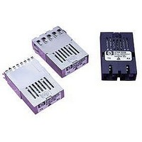
... Ordering Information 850 nm VCSEL (Short Wavelength Laser) AFBR-53D3Z No shield, plastic housing. AFBR-53D3EZ Extended/protruding shield. AFBR-53D3FZ Flush shield. For product information and a complete list of distributors, please go to our web site: Avago, Avago Technologies, and the A logo are trademarks of Avago Technologies, Limited in the United States and other countries. ...