AFBR-5103PEZ Avago Technologies US Inc., AFBR-5103PEZ Datasheet - Page 18
AFBR-5103PEZ
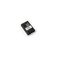
Manufacturer Part Number
AFBR-5103PEZ
Description
TXRX 127MBD DUPLEX SC 1X9 MEZZ
Manufacturer
Avago Technologies US Inc.
Datasheet
1.AFBR-5103TZ.pdf
(20 pages)
Specifications of AFBR-5103PEZ
Data Rate
100Mbps
Wavelength
1308nm
Applications
Ethernet
Voltage - Supply
4.75 V ~ 5.25 V
Connector Type
SC
Mounting Type
Through Hole
Function
Implement FDDI and ATM at the 100 Mbps/125 MBd rate
Product
Transceiver
Pulse Width Distortion
0.02 ns
Maximum Output Current
50 mA
Operating Supply Voltage
4.75 V to 5.25 V
Maximum Operating Temperature
+ 70 C
Minimum Operating Temperature
0 C
Package / Case
SIP-9
For Use With
Multimode Glass
Lead Free Status / RoHS Status
Lead free / RoHS Compliant


AFBR-5103Z/-5103TZ
Receiver Optical and Electrical Characteristics
(T
1
Notes:
Input Optical Power Minimum at
Window Edge
Input Optical Power Minimum at
Eye Center
Input Optical Power Maximum
Operating Wavelength
Duty Cycle Distortion Contributed
by the Receiver
Data Dependent Jitter Contributed
by the Receiver
Random Jitter Contributed by the
Receiver
Signal Detect - Asserted
Signal Detect - Deasserted
Signal Detect - Hysteresis
Signal Detect Assert Time (off to
on)
SignalDetectAssert Time (off to on)
for -40°C to 0°C
Signal Detect Deassert Time (on
to off )
1. This is the maximum voltage that can be applied across the Differen-
2. The outputs are terminated with 50 ý connected to V
3. The power supply current needed to operate the transmitter is
4. This value is measured with the outputs terminated into 50 ý con-
5. The power dissipation value is the power dissipated in the receiver
6. These values are measured with respect to V
7. The output rise and fall times are measured between 20% and 80%
8. Duty Cycle Distortion contributed by the receiver is measured at
Parameter
A
tial Transmitter Data Inputs to prevent damage to the input ESD
protection circuit.
provided to differential ECL circuitry. This circuitry maintains a nearly
constant current flow from the power supply. Constant current opera-
tion helps to prevent unwanted electrical noise from being generated
and conducted or emitted to neighboring circuitry.
nected to V
average.
itself. Power dissipation is calculated as the sum of the products of
supply voltage and currents, minus the sum of the products of the
output voltages and currents.
terminated into 50 ý connected to V
levels with the output connected to V
the 50% threshold using an IDLE Line State, 125 MBd (62.5 MHz
square-wave), input signal. The input optical power level is -20 dBm
average. See Application Information - Transceiver Jitter Section for
further information.
= 0°C to 70°C, V
CC
- 2 V and an Input Optical Power level of -14 dBm
CC
= 4.75 V to 5.25 V)
CC
CC
- 2 V.
-2 V through 50 ý.
P
P
P
l
DCD
DDJ
RJ
P
P
P
AS_Max
AS_Max
ANS_Max
A
A
IN Min.
IN Min.
IN Max.
D
Symbol
- P
CC
D
with the output
(W)
(C)
CC
-2 V.
Min.
-14
1270
P
-45
1.5
0
0
0
D
+ 1.5 dB
10. Random Jitter contributed by the receiver is specified with an IDLE
11. These optical power values are measured with the following
12. The Extinction Ratio is a measure of the modulation depth of the
9. Data Dependent Jitter contributed by the receiver is specified with
• Over the specified operating voltage and temperature ranges.
• With HALT Line State, (12.5 MHz square-wave), input signal.
• At the end of one meter of noted optical fiber with cladding modes
• The Beginning of Life (BOL) to the End of Life (EOL) optical power
the FDDI DDJ test pattern described in the FDDI PMD Annex A.5. The
input optical power level is -20 dBm average. See Application Informa-
tion - Transceiver Jitter Section for further information.
Line State, 125 MBd (62.5 MHz square-wave), input signal. The input
optical power level is at maximum “P
Information - Transceiver Jitter Section for further information.
conditions:
degradation is typically 1.5 dB per the industry convention for
long wavelength LEDs. The actual degradation observed in Avago
Technologies’ 1300 nm LED products is < 1 dB, as specified in this
data sheet.
removed. The average power value can be converted to a peak power
value by adding 3 dB. Higher output optical power transmitters are
available on special request.
optical signal. The data “0” output optical power is compared to the
data “1” peak output optical power and expressed as a percentage.
With the transmitter driven by a HALT Line State (12.5 MHz square-
wave) signal, the average optical power is measured. The data “1”
-33.5
-34.5
-11.8
0.02
0.35
1.0
2.4
55
55
110
Typ. Max.
-31
-31.8
1380
0.4
1.0
2.14
-33
100
130
350
dBm avg.
dBm avg.
dBm avg.
nm
ns p-p
ns p-p
ns p-p
dBm avg.
dBm avg.
dB
µs
µs
µs
Unit
IN Min.
Reference
Note 19
Figure 11
Note 20
Figure 11
Note 19
Note 8
Note 9
Note 10
Note 21, 22
Figure 12
Note 23, 24
Figure 12
Figure 12
Note 21,
Figure 12
Note 21,
Figure 12
Note 23, 24
Figure 12
(W)”. See Application
Related parts for AFBR-5103PEZ
Image
Part Number
Description
Manufacturer
Datasheet
Request
R

Part Number:
Description:
TXRX OPT OC3 MTRJ SFF 2X5DIP
Manufacturer:
Avago Technologies US Inc.
Datasheet:

Part Number:
Description:
TXRX ETHERNET 125MBD MMF 2X5
Manufacturer:
Avago Technologies US Inc.
Datasheet:

Part Number:
Description:
TXRX OPT SFP DGTL 850NM IND
Manufacturer:
Avago Technologies US Inc.
Datasheet:

Part Number:
Description:
650nm FE Transceiver Eval Kit
Manufacturer:
Avago Technologies US Inc.
Datasheet:

Part Number:
Description:
TXRX OPT SFF 4/2/1GBD 2X7
Manufacturer:
Avago Technologies US Inc.
Datasheet:

Part Number:
Description:
TXRX OPT SFP 4/2/1GBD 850NM
Manufacturer:
Avago Technologies US Inc.
Datasheet:

Part Number:
Description:
TXRX OPT XFP 10GB/S 850NM
Manufacturer:
Avago Technologies US Inc.
Datasheet:

Part Number:
Description:
TXRX OPT 1X9 100MBPS ST EXT TEMP
Manufacturer:
Avago Technologies US Inc.
Datasheet:

Part Number:
Description:
TXRX OPT 1X9 100MBPS SC EXT TEMP
Manufacturer:
Avago Technologies US Inc.
Datasheet:

Part Number:
Description:
TXRX OPT 1X9 100MBPS DUPLEX SC
Manufacturer:
Avago Technologies US Inc.
Datasheet:

Part Number:
Description:
OPTOCOUPLER GATE DRV 2A 16-SOIC
Manufacturer:
Avago Technologies US Inc.
Datasheet:
Part Number:
Description:
OPTOCOUPLER 2CH 2.5A 16-SOIC
Manufacturer:
Avago Technologies US Inc.
Datasheet:

Part Number:
Description:
OPTOCOUPLER GATE DRV 0.4A 16SOIC
Manufacturer:
Avago Technologies US Inc.
Datasheet:

Part Number:
Description:
OPTOCOUPLER 2.0A 250KHZ 8-DIP
Manufacturer:
Avago Technologies US Inc.
Datasheet:

Part Number:
Description:
OPTOCOUPLER 2.0A 250KHZ GW 8-SMD
Manufacturer:
Avago Technologies US Inc.
Datasheet: