LTM4601AEV-1#PBF Linear Technology, LTM4601AEV-1#PBF Datasheet - Page 10
LTM4601AEV-1#PBF
Manufacturer Part Number
LTM4601AEV-1#PBF
Description
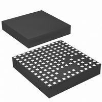
IC DC/DC UMODULE 12A 133-LGA
Manufacturer
Linear Technology
Series
µModuler
Type
Point of Load (POL) Non-Isolatedr
Datasheet
1.LTM4601AEVPBF.pdf
(28 pages)
Specifications of LTM4601AEV-1#PBF
Design Resources
LTM4601A-1 Spice Model
Output
0.6 ~ 5 V
Number Of Outputs
1
Power (watts)
60W
Mounting Type
Surface Mount
Voltage - Input
4.5 ~ 20V
Package / Case
133-LGA
1st Output
0.6 ~ 5 VDC @ 12A
Size / Dimension
0.59" L x 0.59" W x 0.11" H (15mm x 15mm x 2.8mm)
Power (watts) - Rated
60W
Operating Temperature
-40°C ~ 85°C
Efficiency
95%
Lead Free Status / RoHS Status
Lead free / RoHS Compliant
3rd Output
-
2nd Output
-
Available stocks
Company
Part Number
Manufacturer
Quantity
Price


APPLICATIONS INFORMATION
LTM4601A/LTM4601A-1
The typical LTM4601A application circuit is shown in
Figure 18. External component selection is primarily
determined by the maximum load current and output
voltage. Refer to Table 2 for specifi c external capacitor
requirements for a particular application.
V
There are restrictions in the maximum V
down ratio that can be achieved for a given input voltage.
These constraints are shown in the Typical Performance
Characteristics curves labeled “V
Ratio”. Note that additional thermal derating may apply. See
the Thermal Considerations and Output Current Derating
section of this data sheet.
Output Voltage Programming and Margining
The PWM controller has an internal 0.6V reference voltage.
As shown in the Block Diagram, a 1M and a 60.4k 0.5%
internal feedback resistor connects V
together. The V
and the 60.4k resistor. The 1M resistor is used to protect
against an output overvoltage condition if the V
pin is not connected to the output, or if the remote sense
amplifi er output is not connected to V
voltage will default to 0.6V. Adding a resistor R
V
Table 1. R
10
V
R
(kΩ)
IN
FB
(V)
OUT
SET
V
to V
pin to SGND pin programs the output voltage:
OUT
Open
OUT
0.6
= 0.6V
SET
Standard 1% Resistor Values vs V
Step-Down Ratios
60.4
1.2
OUT_LCL
60.4k + R
R
40.2
1.5
SET
pin is connected between the 1M
SET
30.1
1.8
25.5
IN
2
to V
OUT_LCL
OUT
19.1
2.5
IN
OUT
OUT
and V
and V
. The output
SET
13.3
Step-Down
3.3
OUT
from the
OUT_LCL
FB
8.25
step
pins
5
The MPGM pin programs a current that when multiplied
by an internal 10k resistor sets up the 0.6V reference ±
offset for margining. A 1.18V reference divided by the
RPGM resistor on the MPGM pin programs the current.
Calculate V
where %V
and V
where R
pin to ground.
The output margining will be ± margining of the value.
This is controlled by the MARG0 and MARG1 pins. See
the truth table below:
Input Capacitors
LTM4601A module should be connected to a low AC
impedance DC source. Input capacitors are required to
be placed adjacent to the module. In Figure 18, the 10μF
ceramic input capacitors are selected for their ability to
handle the large RMS current into the converter. An input
bulk capacitor of 100μF is optional. This 100μF capacitor is
only needed if the input source impedance is compromised
by long inductive leads or traces.
R
V
OUT(MARGIN)
PGM
OUT(MARGIN)
MARG1
HIGH
HIGH
LOW
LOW
PGM
=
OUT
OUT(MARGIN)
V
0.6V
OUT
is the resistor value to place on the MPGM
is the percentage of V
=
•
is the margin quantity in volts:
V
%V
OUT(MARGIN)
100
1.18V
OUT
:
MARG0
HIGH
HIGH
LOW
LOW
• V
OUT
• 10k
OUT
you want to margin,
MARGIN DOWN
NO MARGIN
MARGIN UP
NO MARGIN
MODE
4601afb
Related parts for LTM4601AEV-1#PBF
Image
Part Number
Description
Manufacturer
Datasheet
Request
R

Part Number:
Description:
IC DC/DC UMODULE 12A 133-LGA
Manufacturer:
Linear Technology
Datasheet:

Part Number:
Description:
12A DC/DC ?Modules with PLL, Output Tracking and Margining
Manufacturer:
LINER [Linear Technology]
Datasheet:
Part Number:
Description:
Low VIN, 8A DC/DC ?Module Regulator
Manufacturer:
LINER [Linear Technology]
Datasheet:

Part Number:
Description:
BOARD EVAL LTM4601
Manufacturer:
Linear Technology
Datasheet:

Part Number:
Description:
IC DC/DC UMODULE 12A 118-LGA
Manufacturer:
Linear Technology
Datasheet:

Part Number:
Description:
IC DC/DC UMODULE 12A 118-LGA
Manufacturer:
Linear Technology
Datasheet:

Part Number:
Description:
IC DC/DC UMODULE 12A 118-LGA
Manufacturer:
Linear Technology
Datasheet:

Part Number:
Description:
IC DC/DC UMODULE 12A 118-LGA
Manufacturer:
Linear Technology
Datasheet:
Part Number:
Description:
CD ROM LINEARVIEW DATASHEETS
Manufacturer:
Linear Technology

Part Number:
Description:
Standalone Linear Li-Ion Battery Charger with Thermal Regulation in ThinSOT
Manufacturer:
Linear Technology Corporation
Datasheet:
Part Number:
Description:
Low noise, high frequency, 8th order linear phase lowpass filter
Manufacturer:
Linear Technology Corporation
Datasheet:
Part Number:
Description:
Manufacturer:
Linear Technology Corporation
Datasheet:
Part Number:
Description:
Manufacturer:
Linear Technology Corporation
Datasheet:
Part Number:
Description:
Manufacturer:
Linear Technology Corporation
Datasheet:
Part Number:
Description:
Manufacturer:
Linear Technology Corporation
Datasheet: