LTM4601AEV-1#PBF Linear Technology, LTM4601AEV-1#PBF Datasheet - Page 7
LTM4601AEV-1#PBF
Manufacturer Part Number
LTM4601AEV-1#PBF
Description
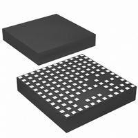
IC DC/DC UMODULE 12A 133-LGA
Manufacturer
Linear Technology
Series
µModuler
Type
Point of Load (POL) Non-Isolatedr
Datasheet
1.LTM4601AEVPBF.pdf
(28 pages)
Specifications of LTM4601AEV-1#PBF
Design Resources
LTM4601A-1 Spice Model
Output
0.6 ~ 5 V
Number Of Outputs
1
Power (watts)
60W
Mounting Type
Surface Mount
Voltage - Input
4.5 ~ 20V
Package / Case
133-LGA
1st Output
0.6 ~ 5 VDC @ 12A
Size / Dimension
0.59" L x 0.59" W x 0.11" H (15mm x 15mm x 2.8mm)
Power (watts) - Rated
60W
Operating Temperature
-40°C ~ 85°C
Efficiency
95%
Lead Free Status / RoHS Status
Lead free / RoHS Compliant
3rd Output
-
2nd Output
-
Available stocks
Company
Part Number
Manufacturer
Quantity
Price


PIN FUNCTIONS
V
tween these pins and PGND pins. Recommend placing
input decoupling capacitance directly between V
and PGND pins.
V
between these pins and PGND pins. Recommend placing
output decoupling capacitance directly between these pins
and PGND pins. Review the fi gure below.
PGND (Bank 2): Power ground pins for both input and
output returns.
V
This pin connects to the ground remote sense point. The
remote sense amplifi er is used for V
NC1 (Pin M12): No Connect On the LTM4601A-1.
V
This pin connects to the output remote sense point. The
remote sense amplifi er is used for V
NC2 (Pin J12): No Connect On the LTM4601A-1.
DIFFV
fi er. This pin connects to the V
NC3 (Pin K12): No Connect On the LTM4601A-1.
DRV
for powering the internal MOSFET drivers. This pin can
be biased up to 6V from an external supply with about
50mA capability, or an external circuit shown in Figure 16.
This improves effi ciency at the higher input voltages by
reducing power dissipation in the module.
IN
OUT
OSNS
OSNS
(Bank 1): Power Input Pins. Apply input voltage be-
CC
(Bank 3): Power Output Pins. Apply output load
–
+
OUT
(Pin E12): This pin normally connects to INTV
(Pin M12): (–) Input to the Remote Sense Amplifi er.
(Pin J12): (+) Input to the Remote Sense Amplifi er.
BANK 1
BANK 2
BANK 3
PGND
V
(Pin K12): Output of the Remote Sense Ampli-
OUT
V
IN
M
A
B
C
D
E
G
H
K
L
F
J
1
2 3 4 5 6 7
*LTM4601A-1 ONLY
TOP VIEW
(See Package Description for Pin Assignment)
INTV
OUT_LCL
CC
8 9 10 11 12
MTP1
MTP2
MTP3
OUT
OUT
pin.
≤3.3V.
≤3.3V.
f
MARG0
MARG1
DRV
V
PGOOD
SGND
V
DIFFV
V
V
SET
FB
OSNS
OUT_LCL
OSNS
CC
OUT
+
–
/NC2*
/NC1*
/NC3*
IN
pins
CC
INTV
of the 5V internal regulator. These pins are internally
connected. Pin A7 is a test pin.
PLLIN (Pin A8): External Clock Synchronization Input to
the Phase Detector. This pin is internally terminated to
SGND with a 50k resistor. Apply a clock above 2V and
below INTV
TRACK/SS (Pin A9): Output Voltage Tracking and Soft-
Start Pin. When the module is confi gured as a master
output, then a soft-start capacitor is placed on this pin
to ground to control the master ramp rate. A soft-start
capacitor can be used for soft-start turn on as a stand
alone regulator. Slave operation is performed by putting
a resistor divider from the master output to the ground,
and connecting the center point of the divider to this pin.
See Applications Information.
MPGM (Pins A12, B11): Programmable Margining Input.
A resistor from this pin to ground sets a current that is
equal to 1.18V/R. This current multiplied by 10kΩ will
equal a value in millivolts that is a percentage of the 0.6V
reference voltage. See Applications Information. To parallel
LTM4601As, each requires an individual MPGM resistor.
Do not tie MPGM pins together. Both pins are internally
connected. Pin A12 is a test pin.
f
An external resistor can be placed from this pin to ground
to increase frequency. This pin can be decoupled with a
1000pF capacitor. See Applications Information for fre-
quency adjustment. Both pins are internally connected.
Pin B12 is a test pin.
V
Internally, this pin is connected to V
60.4k precision resistor. Different output voltages can be
programmed with an additional resistor between V
SGND pins. See Applications Information.
MARG0 (Pin C12): This pin is the LSB logic input for the
margining function. Together with the MARG1 pin will
determine if margin high, margin low or no margin state
is applied. The pin has an internal pull-down resistor of
50k. See Applications Information.
SET
FB
(Pin F12): The Negative Input of the Error Amplifi er.
(Pins B12, C11): Frequency Set Internally to 850kHz.
CC
(Pin A7, D9): This pin is for additional decoupling
LTM4601A/LTM4601A-1
CC
. See Applications Information.
OUT_LCL
pin with a
FB
4601afb
and
7
Related parts for LTM4601AEV-1#PBF
Image
Part Number
Description
Manufacturer
Datasheet
Request
R

Part Number:
Description:
IC DC/DC UMODULE 12A 133-LGA
Manufacturer:
Linear Technology
Datasheet:

Part Number:
Description:
12A DC/DC ?Modules with PLL, Output Tracking and Margining
Manufacturer:
LINER [Linear Technology]
Datasheet:
Part Number:
Description:
Low VIN, 8A DC/DC ?Module Regulator
Manufacturer:
LINER [Linear Technology]
Datasheet:

Part Number:
Description:
BOARD EVAL LTM4601
Manufacturer:
Linear Technology
Datasheet:

Part Number:
Description:
IC DC/DC UMODULE 12A 118-LGA
Manufacturer:
Linear Technology
Datasheet:

Part Number:
Description:
IC DC/DC UMODULE 12A 118-LGA
Manufacturer:
Linear Technology
Datasheet:

Part Number:
Description:
IC DC/DC UMODULE 12A 118-LGA
Manufacturer:
Linear Technology
Datasheet:

Part Number:
Description:
IC DC/DC UMODULE 12A 118-LGA
Manufacturer:
Linear Technology
Datasheet:
Part Number:
Description:
CD ROM LINEARVIEW DATASHEETS
Manufacturer:
Linear Technology

Part Number:
Description:
Standalone Linear Li-Ion Battery Charger with Thermal Regulation in ThinSOT
Manufacturer:
Linear Technology Corporation
Datasheet:
Part Number:
Description:
Low noise, high frequency, 8th order linear phase lowpass filter
Manufacturer:
Linear Technology Corporation
Datasheet:
Part Number:
Description:
Manufacturer:
Linear Technology Corporation
Datasheet:
Part Number:
Description:
Manufacturer:
Linear Technology Corporation
Datasheet:
Part Number:
Description:
Manufacturer:
Linear Technology Corporation
Datasheet:
Part Number:
Description:
Manufacturer:
Linear Technology Corporation
Datasheet: