UM245R FTDI, Future Technology Devices International Ltd, UM245R Datasheet - Page 9
UM245R
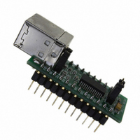
Manufacturer Part Number
UM245R
Description
MODULE USB-PAR FIFO TTL 24-DIP
Manufacturer
FTDI, Future Technology Devices International Ltd
Datasheet
1.UM245R.pdf
(27 pages)
Specifications of UM245R
Main Purpose
Interface, USB 2.0 to Parallel FIFO Bridge
Embedded
No
Utilized Ic / Part
FT245R
Primary Attributes
300kBps to 1MBps USB to parallel FIFO via 4-Wire Interface
Secondary Attributes
Royalty-Free Drivers
Lead Free Status / RoHS Status
Lead free / RoHS Compliant
Other names
768-1020


4.2 Signal Descriptions
Pin No.
1
2
3
4
5
6
7, 24
8
9
10
11
12
13
14
15, 21
17
16
19
20
18
© Copyright 2009 Future Technology Devices International Ltd
Name
DB0
DB4
DB2
VIO
DB1
DB7
GND
DB5
DB6
DB3
PWE#
RD#
SLD
USB
VCC
PU1
PU2
3V3
RST#
WR
Type
I/O
I/O
I/O
PWR
I/O
I/O
PWR
I/O
I/O
I/O
I/O
I/O
GND
Output
PWR
or
Output
Control
Control
Output
Input
I/O
Description
FIFO Data Bus Bit 0*
FIFO Data Bus Bit 4*
FIFO Data Bus Bit 2*
+1.8V to +5.25V supply to the FIFO Interface and Control group pins (1...3, 5, 6,
9...14, 22, 23).
In USB bus powered designs connect to 3V3OUT to drive out at 3.3V levels (connect
jumper J1 pins 1 and 2 together), or connect to VCC to drive at 5V CMOS level (connect
jumper J1 pins 2 and 3 together). This pin can also be supplied with an external 1.8V –
5.0V supply in order to drive at different levels. It should be noted that in this case this
supply should originate from the same source as the supply to Vcc. This means that in
bus powered designs a regulator which is supplied by the 5V on the USB bus should be
used.
FIFO Data Bus Bit 1*
FIFO Data Bus Bit 7*
Module ground supply pins
FIFO Data Bus Bit 5*
FIFO Data Bus Bit 6*
FIFO Data Bus Bit 3*
Goes low after the device is configured by USB, then high during USB suspend. Can be
used to control power to external logic P-Channel logic level MOSFET switch. Enable the
interface pull-down option when using the PWREN# pin in this way.
Enables the current FIFO data byte on D0...D7 when low. Fetched the next FIFO data
byte (if available) from the receive FIFO buffer when RD# goes from high to low. See
Section 4.4
USB Cable shield.
5V Power output USB port. For a low power USB bus powered design, up to 100mA can
be sourced from the 5V supply on the USB bus. A maximum of 500mA can be sourced
from the USB bus in a high power USB bus powered design.
These two pins are internally connected on the module PCB. To power the module from
the 5V supply on USB bus, connect jumper J2 pins 1 and 2 together (this is the module
default configuration). In this case these pins would have the same description as pin
14.
To use the UM245R module in a self powered configuration, ensure that jumper J2 pins
1 and 2 are not connected together, and apply an external 3.3V to 5.25V supply to one
or both of these pins.
Pull up resistor pin connection 2. Connect to pin 17 (RST#) in a self powered
configuration.
Pull up resistor pin connection 1. Connect to pin 14 (USB) in a self powered
configuration.
3.3V output from integrated LDO regulator. This pin is decoupled to ground on the
module PCB with a 100nF capacitor. The prime purpose of this pin is to provide the
internal 3.3V supply to the USB transceiver cell and the internal 1.5kΩ pull up resistor
on USBDP. Up to 50mA can be drawn from this pin to power external logic if required.
This pin can also be used to supply the FT245RL‟s VCCIO pin by connecting this pin to
pin 4 (VIO), or by connecting together pins 1 and 2 on jumper J1.
Can be used by an external device to reset the FT245R. If not required can be left
unconnected, or pulled up to VCCIO.
Writes the data byte on the D0...D7 pins into the transmit FIFO buffer when WR goes
from high to low. See
UM245R USB - Parallel FIFO Development Module Datasheet Version 1.04
for timing diagram.*
Section 4.4
for timing diagram.*
Document Reference No.: FT_000202
Clearance No.: FTDI# 124
8
Related parts for UM245R
Image
Part Number
Description
Manufacturer
Datasheet
Request
R

Part Number:
Description:
IC USB TO SERIAL UART 32-QFN
Manufacturer:
FTDI, Future Technology Devices International Ltd

Part Number:
Description:
IC USB HOST CTLR VINCULUM 48LQFP
Manufacturer:
FTDI, Future Technology Devices International Ltd
Datasheet:

Part Number:
Description:
IC USB HOST VINCULUM-II 32QFN
Manufacturer:
FTDI, Future Technology Devices International Ltd
Datasheet:
Part Number:
Description:
IC USB HOST VINCULUM-II 32LQFN
Manufacturer:
FTDI, Future Technology Devices International Ltd
Datasheet:
Part Number:
Description:
IC USB HOST VINCULUM-II 48QFN
Manufacturer:
FTDI, Future Technology Devices International Ltd
Datasheet:
Part Number:
Description:
IC USB HOST VINCULUM-II 32LQFN
Manufacturer:
FTDI, Future Technology Devices International Ltd
Datasheet:
Part Number:
Description:
IC USB HOST VINCULUM-II 32QFN
Manufacturer:
FTDI, Future Technology Devices International Ltd
Datasheet:
Part Number:
Description:
IC USB HOST VINCULUM-II 48LQFP
Manufacturer:
FTDI, Future Technology Devices International Ltd
Datasheet:
Part Number:
Description:
IC USB HOST VINCULUM-II 48LQFP
Manufacturer:
FTDI, Future Technology Devices International Ltd
Datasheet:
Part Number:
Description:
IC USB HOST VINCULUM-II 48QFN
Manufacturer:
FTDI, Future Technology Devices International Ltd
Datasheet:
Part Number:
Description:
IC USB HOST CTLR VINCULUM 64QFN
Manufacturer:
FTDI, Future Technology Devices International Ltd
Datasheet:

Part Number:
Description:
IC USB HOST CTLR VINCULUM 64LQFP
Manufacturer:
FTDI, Future Technology Devices International Ltd
Datasheet:
Part Number:
Description:
IC USB HOST VINCULUM-II 64LQFP
Manufacturer:
FTDI, Future Technology Devices International Ltd
Datasheet:
Part Number:
Description:
IC USB HOST VINCULUM-II 64QFN
Manufacturer:
FTDI, Future Technology Devices International Ltd
Datasheet:

Part Number:
Description:
IC USB TO PARALLEL FIFO 28-SSOP
Manufacturer:
FTDI, Future Technology Devices International Ltd
Datasheet: