ATWEBDVK-02VOIP Atmel, ATWEBDVK-02VOIP Datasheet - Page 67
ATWEBDVK-02VOIP
Manufacturer Part Number
ATWEBDVK-02VOIP
Description
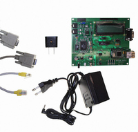
KIT DEV TCP/IP AT89C51RD2 VOIP
Manufacturer
Atmel
Series
@Webr
Datasheet
1.ATWEBDVK-02RC.pdf
(137 pages)
Specifications of ATWEBDVK-02VOIP
Main Purpose
*
Embedded
*
Utilized Ic / Part
AT89C51RD2
Primary Attributes
*
Secondary Attributes
*
Lead Free Status / RoHS Status
Contains lead / RoHS non-compliant


Figure 16-4. Data Transmission Format (CPHA = 0)
Figure 16-5. Data Transmission Format (CPHA = 1)
Figure 16-6. CPHA/SS Timing
16.3.3
4235K–8051–05/08
Error Conditions
MOSI (from Master)
SCK Cycle Number
MISO (from Slave)
MOSI (from Master)
SCK (CPOL = 0)
SCK (CPOL = 1)
MISO (from Slave)
SCK Cycle Number
SPEN (Internal)
SCK (CPOL = 0)
SCK (CPOL = 1)
Capture Point
SPEN (Internal)
SS (to Slave)
Capture Point
SS (to Slave)
As shown in
must begin driving its data before the first SCK edge, and a falling edge on the SS pin is used to
start the transmission. The SS pin must be toggled high and then low between each Byte trans-
mitted (Figure 16-6).
Figure 16-5
driving its MOSI pin on the first SCK edge. Therefore, the Slave uses the first SCK edge as a
start transmission signal. The SS pin can remain low between transmissions
format may be preferred in systems having only one Master and only one Slave driving the
MISO data line.
The following flags in the SPSTA signal SPI error conditions:
MISO/MOSI
(CPHA = 0)
(CPHA = 1)
Master SS
Slave SS
Slave SS
shows an SPI transmission in which CPHA is ’1’. In this case, the Master begins
Figure
MSB
MSB
MSB
1
MSB
1
16-4, the first SCK edge is the MSB capture strobe. Therefore, the Slave
2
bit6
bit6
2
bit6
Byte 1
bit6
3
bit5
bit5
3
bit5
bit5
bit4
4
bit4
bit4
4
bit4
Byte 2
bit3
bit3
5
bit3
bit3
5
6
bit2
bit2
6
bit2
bit2
Byte 3
7
bit1
bit1
7
bit1
bit1
AT89C51RD2/ED2
LSB
8
LSB
LSB
8
LSB
(Figure
16-6). This
67
Related parts for ATWEBDVK-02VOIP
Image
Part Number
Description
Manufacturer
Datasheet
Request
R

Part Number:
Description:
KIT DEV TCP/IP AT89C51RD2
Manufacturer:
Atmel
Datasheet:

Part Number:
Description:
KIT DEV TCP/IP AT89C51RD2 REMOTE
Manufacturer:
Atmel
Datasheet:

Part Number:
Description:
KIT DEV TCP/IP AT89C51RD2 WEBCAM
Manufacturer:
Atmel
Datasheet:

Part Number:
Description:
DEV KIT FOR AVR/AVR32
Manufacturer:
Atmel
Datasheet:

Part Number:
Description:
INTERVAL AND WIPE/WASH WIPER CONTROL IC WITH DELAY
Manufacturer:
ATMEL Corporation
Datasheet:
Part Number:
Description:
Low-Voltage Voice-Switched IC for Hands-Free Operation
Manufacturer:
ATMEL Corporation
Datasheet:
Part Number:
Description:
MONOLITHIC INTEGRATED FEATUREPHONE CIRCUIT
Manufacturer:
ATMEL Corporation
Datasheet:
Part Number:
Description:
AM-FM Receiver IC U4255BM-M
Manufacturer:
ATMEL Corporation
Datasheet:
Part Number:
Description:
Monolithic Integrated Feature Phone Circuit
Manufacturer:
ATMEL Corporation
Datasheet:
Part Number:
Description:
Multistandard Video-IF and Quasi Parallel Sound Processing
Manufacturer:
ATMEL Corporation
Datasheet:
Part Number:
Description:
High-performance EE PLD
Manufacturer:
ATMEL Corporation
Datasheet:
Part Number:
Description:
8-bit Flash Microcontroller
Manufacturer:
ATMEL Corporation
Datasheet: